Xilinx has continued to increase its performance to match the increasing demands of target applications. The giant tech company continues to design new innovations. As Xilinx improves the architecture of the Virtex, the number of logic keeps increasing.
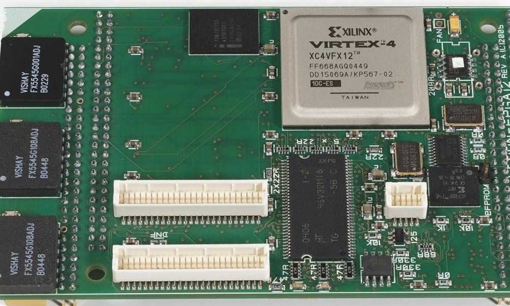
The Virtex-4 FPGA by Xilinx facilitates programmable logic design capabilities. The Xilinx Virtex-4 FPGA is a great alternative to ASIC technology. This FPGA features three basic platform families which are FX, LX, and SX. Also, these platforms offer combinations and options to address all complicated applications.
Xilinx Virtex-4 FPGA – What is it?
Xilinx Virtex-4 FPGA was formally introduced in June 2004. It features a programmable logic solution that meets the needs of designers. The Virtex-4 FPGA building blocks are the upgraded version of previous Virtex versions. Therefore, previous versions are upward compatible.
Virtex-4 FPGAs feature several embedded cores and configurable elements for high-performance system designs.
Features of Xilinx Virtex-4 FPGA
This user-programmable gate array offers a lot of features. These features include:
Input/Output Blocks
I/O blocks have the interface between the internal configurable logic and package pins. Also, IOBs are specifically enhanced for source-synchronous devices. I/O blocks have different categories like:
- Per-bit deskew circuitry
- Output block with a DDR or SDR register
- Bidirectional block
- Regional clocking resources and Dedicated I/O
- In-built data deserializer/ serializer
- Programmable differential or single-ended operation
IOBs provide support for these single-ended standards:
- GTLP and GTL
- LVCMOS
- PCI-X
- LVTTL
- PCI (66 and 33 MHz)
- SSTL 2.5V and 1.8V
Also, IOBs can support differential signaling I/O standards like:
- ULVDS
- LVDS
- Differential SSTL 2.5V and 1.8V
- BLVDS
- Differential HSTL 1.8V and 1.5V
——————————————————————————————————————
Request Xilinx Virtex-4 FPGA Quote, Pls Send Files to Sales@raypcb.com Now
——————————————————————————————————————
Block RAM
The block RAM can use large embedded storage blocks. The resources here are 18Kb true dual-port RAM blocks.
Boundary Scan
This supports a standard technique for configuring and assessing Virtex-4 devices. Also, the boundary scan complies with IEEE standards 1532 and 1149.1.
Global clocking
This features a lasting solution for creating high-speed clock networks. There are about twenty DCM blocks available. Also, there are about 32 global-clock MUX buffers in Virtex-4.
Configurable Logic Blocks (CLBs)
A CLB features about four slices. Each slice comprises:
- Two storage elements
- Large multiplexers
- Two function generators
- Arithmetic logic gates
- Fast carry look-ahead chain
Configuration
Xilinx Virtex-4 FPGA’s configuration uses some modes to load the bitstream into internal configuration memory. These modes include:
- Slave SelectMAP mode
- Slave-serial mode
- Boundary-Scan mode
- Master SelectMAP mode
- Master-serial mode
Routing resources
Virtex 4 devices feature some components. These components utilize the same interconnect scheme. Also, the timing models improve the performance of high-performance designs.
Xilinx Virtex-4 FPGA’s Block RAM
In this FPGA, every block RAM stores 18Kbits of data. The size of the Virtex-4 device will determine the number of block RAM memory. Also, the 18 Kbit blocks can allow a wider and deeper memory implementation.
Features of Block RAM in Virtex-4
Independent read and write port width selection
Block RAM ports can control address depth and data width. Virtex-4 devices enable Read and Write to be configured with separate data width. This width selection helps to efficiently implement a CAM in block RAM. CAM means content addressable memory.
Byte-Wide write enable
This helps to write 8 bit portions of incoming data. Block RAM features four different byte-write enable inputs. Every byte-write enable is related with one parity bit and one byte of input data. Also, Byte-wide write enable feature helps to interface Block RAM with the PPC405. This feature isn’t available in the Multi-rate FIFO.
Cascadable Block RAM
In Virtex-4 Block Ram, you can combine two 16Kbit x 1 RAM to create a 32K x 1 RAM. You can do this without the need for additional CLB logic resources or local interconnect. The 32Kbit x 1 RAM doesn’t support the NO_CHANGE mode. Also, you can only increase the depth of the block RAM in the 32K x 1 mode.
Optional Output Registers
These enhance design performance by removing routing delay to the CLB flip-flops. These output registers feature programmable clock inversion. Also, there is an independent clock enabling input for these registers.
Block RAM Port Signals
Every block RAM port functions independently of other ports. Some of the block RAM port signals include:
- Enable-EN[A|B]
- Register Enable – REGCE[A|B]
- Address Bus- ADDR[AIB] <14:#>
- Write Enable – WE[A|B]
- Clock – CLK[A|B]
- Data-In Buses – DI[A|B]<#:0> & DIP[A|B]<#:0>
The Configurable Logic Blocks (CLBs) of Xilinx Virtex-4 FPGA
CLBs are the basic logic resource for performing combinatorial circuits and sequential. Also, every CLB element connects to a switch matrix. This helps to gain access to the general routing matrix. There are four different interconnected slices in a CLB, These slices are in pairs. Every pair is carefully arranged as a column.
SLICEL specifies the pair of slices in the right column. Also, there is SLICEM, which specifies the pair of slices in the left column. There is an independent carry chain for every pair in a column. But, the slices in SLICEM feature a common shift chain.
According to the Xilinx tools, when a number follows an “X,” it specifies a column of slices. When a number follows “Y,” this specifies the position of every slice in a pair.
Description of SLICE
Some elements are common to SLICEL and SLICEM. These elements are:
- Two storage elements
- Arithmetic gates
- Two look-up tables
- carry logic
- Wide-function multiplexers
Storage elements
Virtex-4 FPGA slice features storage elements. These elements can configure as level-sensitive latches or D-type flip-flops. LUT output can drive the D input through the DY or DX multiplexer. The Clock Enable, Control Signals Clock, and the Set/Reset are common to these elements. Also, there is independent polarity in all control signals.
Any inverter on a control input becomes automatically absorbed. By default, the clock-enable signal is High. The clock enable goes to the active state if left unconnected. Furthermore, every slice features reset and set signals. The set/reset compels the storage element into the condition specified by SRLow or SRHigh.
——————————————————————————————————————
Request Xilinx Virtex-4 FPGA Quote, Pls Send Files to Sales@raypcb.com Now
——————————————————————————————————————
Arithmetic Logic
This features an XOR gate that enables the implementation of a 2-bit full adder within a slice. Also, a dedicated GAND and FAND gate enhance the capability of multiplier implementation.
Look-UP Table
The two function generators in a slice feature four independent inputs each. The function generators can implement any arbitrarily defined four-input Boolean function.
Carry Logic
This offers fast arithmetic subtraction and addition. The CLB in Virtex-4 FPGA comprises two distinct carry chains. These chains have a height of two bits per slice. Virtex-4 device’s carry chain is running upward. You can also use the carry multiplexer and dedicated carry path to cascade function generators.
Multiplexers
The associated multiplexers and function generators in Virtex-4 FPGA can implement these:
- 8:1 multiplexer in two slices
- 16:1 multiplexer in four slices
- 4:1 multiplexer in one slice
- 32:1 multiplexer in eight slices
Wide input multiplexers are carefully used in one level of logic. Also, every slice features one MUFTX multiplexer and MUXF5 multiplexer. MUXFX multiplexer uses the MUXF8, MUXF7, and MUXF6. MUXFX can allow combining LUT of about 16 LUTs. You can implement a 2:1 multiplexer for any LUT.
Global Clocking Resources in Xilinx Virtex-4 FPGA
Global clocks are a network of interconnects designed to get to all clock inputs. These networks are specifically designed to feature low skew and increased jitter tolerance. Also, they can support high frequency signals. The global clocking resources comprise some components and paths:
- Clock regions
- Global clock inputs
- Clock tree and nets
- Global clock buffers
Clock Regions
The clock regions help to enhance the clocking distribution in Virtex-4 devices. Every clock region can feature about eight global clock domains. The combination of the thirty-two global clock buffers can help to drive these clock domains. In Virtex-4 FPGA, a clock region can’t be restricted to four quadrants irrespective of the device size. Xilinx Virtex-4 FPGA can support more multiple clock domains.
Global clock inputs
There are global clock inputs location used as regular user I/Os in Virtex-4. The device size determines the number of clock inputs. For instance, smaller devices comprise 16 clock inputs. Larger devices contain 32 clock inputs. The larger the device, the more the number of clock inputs.
You can configure clock inputs for any I/O standard. Every clock input can either be differential or single-ended. Also, all 32 or 16 clock inputs can be made differential. You can configure global clock input pins for any output standard. However, the HT ad LVDS output differential standards are an exception to this. Every global clock input pin provides support for any single-ended output standard.
Clock tree and nets
The clock trees in Virtex-4 are specifically designed for low-power operation. If there is an unused branch in this tree, it will be fully disconnected. Also, the clock trees manage the fanout when you have used the logic resources. All buffers and global clock lines are differentially implemented. This enhances better duty cycles and rejects common-mode noise.
This FPGA doesn’t limit the pin access of the global clock lines to the logic resources pins. Also, the global clock lines can have access to other CLB pins. This architecture is ideal for applications demanding fast signal connection.
Global Clock Buffers
Each Virtex-4 device features 32 global clock buffers. Each half comprises 16 global clock buffers. Global clock buffers enable signal/clock resources to access the global clock trees. The input sources for the global clock buffers are:
- General interconnect
- Digital Clock Manager
- Global clock input
- Rocket IO Multi-Gigabit Transceivers
- Phase-matched clock divider outputs
All global clock buffers can configure as an asynchronous or synchronous “glitch free.” There are more control pins in Virtex-4 devices. This helps to offer enhanced input switching and better functionality.
Regional Clocking Resources in Xilinx Virtex-4 FPGA
The regional clock is independent of the global clock resources. Also, the span of this clock signal features three clock regions. The regional clocking resources in Virtex-4 comprise these paths:
- Regional clock nets
- Clock capable I/O
- Regional clock buffer
- I/O clock buffer
Regional clock nets
These clock nets are ideal for low-power and low-skew operation. Also, these nets manage the fanout when all logic resources are in use. Regional clock nets are specifically restricted to one clock region. There are two independent regional clock nets in one clock region. You must instantiate BUFRs to have access to these nets.
Clock Capable I/O
A clock region features two clock capable I/O pin pairs. In each bank, there are four dedicated clock capable I/O sites. Clock-capable pins have the ability to drive BUFR and BUFIO. However, they can’t connect directly to the global clock buffers.
Regional clock buffer
This is a new clock buffer in Virtex-4 devices. Also known as BUFR, this buffer drive clock signals within a clock region. Also, every BUFR is capable of driving the two regional clock nets in its location. This clock buffer can drive logic resources and I/O logic in the adjacent clock regions. A clock region comprises two regional clock buffers.
I/O clock buffer
Also known as BUFIO, I/O clock buffer is a new feature in Virtex-4 devices. The I/O clock buffer drives a clock net within the column of I/O. Also, these buffers are ideal for source-synchronous data capture. They can drive two I/O clock nets and regional clock buffers in the same region. This is because the I/O clock only gets to the I/O column.
The Input/Output Characteristics of Xilinx Virtex-4 FPGA
Xilinx Virtex-4 FPGA comprises configurable SelectIO™ technology receivers and drivers. Also,this technology supports various standard interfaces. Every IOB features 3-state SelectIO drivers, input, and output. You can configure these drivers to different I/O standards. Also, the differential I/O uses two IOBs in one tile.
Every I/O in Virtex-4 FPGA tile features two IOBs. Also, there are two OLOGIC and ILOGIC blocks. Every IOB is directly connected to an OLOGIC/ILOGIC pair. This pair comprises the output and input logic resources for 3-state control for the IOB.
The I/O Bank Rules in Virtex-4 FPGA I/O
The number of banks in this FPGA isn’t restricted to eight unlike other FPGAs. In Virtex-4, an I/O bank comprises 64 IOBs. The device size determines the number of banks. In addition, the device type determines the number of I/O banks. The Virtex-4 FPGA banks generally support 3.3V single-ended I/O standards.
Virtex-4 devices support low-voltage I/O standards. However, the majority of these standards need a different Vcco. Therefore, every device supports many output drive source voltages.
The Digitally Controlled Impedance (DCI) in Virtex-4 FPGA
PC board design becomes more complicated as FPGAs become bigger. Also, it becomes more critical to maintain signal integrity as edge rates become faster. Therefore, you must terminate PC board traces to prevent ringing. You will need to add resistors to terminate a trace. These resistors make the input or output match the driver or receiver’s impedance to that of the trace’s.
However, placing resistors close to the device pins enhances the component count and board area. Also, this can be impossible in some cases. Therefore, Xilinx designed the DCI technology to help achieve improved signal integrity.
Xilinx DCI
DCI controls the driver’s impedance by using two multi-purpose reference pins in every bank. A reference resistor must pull the VRN (N reference pin) to Vcco. Another reference resistor must pull the VRP (P reference pin) to ground. Each reference resistor’s value must be equal to the PC board traces’ characteristic impedance.
When DCI I/O standards aren’t utilized in the bank, the multi-purpose reference pins become regular I/O pins. Also, DCI adjusts the I/O impedance by turning transistors on or off. Here, the impedance must match the external reference resistors. Furthermore, there are two phases in impedance adjustment. The first phase controls large transistors in the I/Os. Therefore, it compensates for any process variations.
The second phase controls the smaller transistors in the I/Os. Therefore, it maintains the impedance based on supply voltage and temperature variations. Also, the second phase starts after the first phase. This phase keeps going on even when the device is functioning.
Adjust the impedance to match the reference resistors. Do this for controlled impedance output drivers. Also, you can adjust the impedance to match half the resistance of the reference resistors. You adjust the termination to match the reference resistors for on-chip termination.
Importance of DCI
Digitally Controlled Impedance (DCI) is a crucial technology in Virtex-4 FPGA. It adjusts the input termination and output impedance. Therefore, these factors will match the characteristics impedance of the transmission line. Also, the I/O impedance is actively adjusted to match external reference resistance. This serves as a compensation for any changes in I/O impedance from process variation.
Also, DCI keeps adjusting the I/O impedance to compensate for temperature variations. DCI matches the driver impedance to reference resistors. In addition, DCI removes any need for external series termination resistors.
This technology offers parallel termination for receivers or transmitters. Therefore, it makes termination resistors on the board not necessary. Also, DCI can minimize board routing challenges and component count. It enhances signal integrity by removing stub reflection. This reflection happens when resistors are far from the transmission line’s end.
I/O Design Guidelines in Virtex-4 FPGA
There are several design techniques and guidelines in virtex-4 FPGA. Also, these guidelines help you achieve great performance. Below are some I/O standard rules in virtex-4:
Undershoot/Overshoot
There are overshoot and undershoot voltages in I/O standards. Overshoot voltages mustn’t go beyond maximum ratings of 4.05V. Undershot voltages must not exceed -0.3V. The value of Vcco directly influences the maximum undershoot value. Xilnx recommends implementing IBIS simulation to verify maximum specifications. Also, proper I/O termination can verify if undershoot and overshoot.
LVDCI_33 and source termination
To reduce undershoot and overshoot, the I/O drivers matches the trace impedance. The DCI features an in-built source termination on output pins. This compensates changes in impedance as a result of temperature changes.
The LVDCI-33 enables the DCI properties for 3.3V I/O operations. The pull-down resistor attached to VRP specifies the output impedance. The pull-up resistor attached to VRN indicates the output impedance of all the output drivers. Also, source termination must be on the driver side. This is because the LVDCI_33 standard has no input termination.
Maintaining Vcco at 3.0V
Another way to manage undershoot and overshoot problems is to regulate Vcco. The power clamp diode becomes 3.5V when you reduce Vcco to 3.0V. Therefore, this restricts any overshoot greater than 3.5V. Also, reducing Vccco to 3.0V helps to address overshoot and undershoot specifications.
——————————————————————————————————————
Request Xilinx Virtex-4 FPGA Quote, Pls Send Files to Sales@raypcb.com Now
——————————————————————————————————————
Virtex-4 FPGA Devices
XC4VSX55-10FFG1148I XC4VSX55-10FFG1148C XC4VSX55-11FFG1148I
XC4VSX55-10FF1148I XC4VSX35-11FFG668I XC4VSX35-12FFG668C
XC4VSX35-10FFG668C XC4VSX35-10FF668I XC4VSX35-10FFG668I
XC4VSX35-10FF668C XC4VLX80-10FF1148C XC4VLX80-12FFG1148C
XC4VLX60-11FFG1148C XC4VLX60-11FF668CES XC4VLX60-FF1148I
XC4VLX60-10FFG1148C XC4VLX60-10FF1148C XC4VLX60-10FF668I
XC4VLX40-11FFG1148I XC4VLX40-11FFG1148C XC4VLX40-12FFG668C
XC4VLX40-11FF1148I XC4VLX40-10FFG668C XC4VLX40-11FF1148C
XC4VLX40-10FFG1148C XC4VLX40-10FF668I XC4VLX40-10FFG1148I
XC4VLX40-10FF668C XC4VLX25-11FFG668C XC4VLX40-10FF1148I
XC4VLX25-11FF668C XC4VLX25-10SFG363I XC4VLX25-11FF668I
XC4VLX25-10SF363C XC4VLX25-10FF668I XC4VLX25-10FFG668I
XC4VLX160-12FF1148C XC4VLX160-10FF1148C XC4VLX200-10FF1513C
XC4VLX15-12FF668C XC4VLX15-10SF363C XC4VLX15-10SF363I
XC4VLX100-10FFG1513I XC4VLX100-10FFG1148C XC4VLX100-11FF1513C
XC4VLX100-10FF1513I XC4VFX60-11FFG672I XC4VLX100-10FF1148C
XC4VFX60-11FFG1152I XC4VFX60-10FFG672C XC4VFX60-11FFG672C
XC4VFX60-10FFG1152C XC4VFX60-10FF672C XC4VFX60-10FF672I
XC4VFX40-10FFG672I XC4VFX20-10FFG672I XC4VFX40-11FFG672C
XC4VFX20-10FFG672C XC4VFX12-10FF668I XC4VFX140-10FFG1517I
XC4VFX100-11FFG1152C XC4VLX60-10FF668M XC4VFX100-11FFG1517I
XC4VLX25-11FF668CES XC4VFX60-FF1152DGQ XC4VLX25-10FG363I
XC4VSX55-12FFG1148C XC4VSX55-12FF1148C XC4VFX40-4FFG672I
XC4VSX55-11FFG1148C XC4VSX55-11FF1148C XC4VSX55-11FF1148I
XC4VSX55-10FF1148C XC4VSX35-12FF668C XC4VSX55-10FFG1148CS2
XC4VSX35-11FFG668C XC4VSX35-11FF668C XC4VSX35-11FF668I
XC4VSX25-11FFG668C XC4VSX25-11FFG668I XC4VSX25-11FF668I
XC4VSX25-11FF668C XC4VSX25-10FFG668C XC4VSX25-10FFG668I
XC4VSX25-10FF668C XC4VLX80-12FF1148C XC4VSX25-10FF668I
XC4VLX80-11FFG1148I XC4VLX80-11FF1148I XC4VLX80-11FFG1148C
XC4VLX80-11FF1148C XC4VLX80-10FFG1148C XC4VLX80-10FFG1148I
XC4VLX80-10FF1148I XC4VLX60-12FFG1148C XC4VLX60-12FFG668C
XC4VLX60-12FF1148C XC4VLX60-11FFG668I XC4VLX60-12FF668C
The devices listed above belong to the Xilinx Virtex-4 FPGA. These devices share some common features. However, they are also features that make them stand out from one another. We will mention the features of some of these devices.
Features of XC4VLX15-10SF363I
The XC4VLX15-10SF363I belongs to the Xilinx Virtex-4 family. This device comes with some features which include:
- Differential global clocks
- PowerPC 405 Core
- Flexible logic resources
- 2V core voltage
- DCI termination
- Digital clock manager blocks
- Optional pipeline stages
- 5V to 3.3V I/O operation
- Fine grained I/O banking
- SelectIO technology
- Flip-Chip packaging
Features of XC4VLX100-10FFG1148C
The Xilinx XC4VLX100-10FFG1148C is a great alternative to ASIC technology. This Virtex-4 device comprises the following features:
- Additional phase-matched clock dividers
- Built-in ChipSync
- 18 x 18, two’ s complement
- 90mm Copper CMOS process
- Differential global clocks
- DCI active termination
- Optional pipeline stages
Conclusion
The Xilinx Virtex-4 FPGA is one of the most efficient field programmable arrays. This FPGA offers several features and advantages.
