KiCad is a popular open-source software suite that is used for designing electronic circuits. It is known for its flexibility, ease of use, and powerful features. The software is available for free and can be downloaded from the official website. It is compatible with Windows, Linux, and macOS, making it accessible to a wide range of users.
One of the key features of KiCad is its schematic capture tool, which allows users to create and edit electronic schematics quickly and easily. The tool is intuitive and user-friendly, and it supports a wide range of circuit elements, including resistors, capacitors, transistors, and more. The software also includes a powerful netlist generator, which can automatically generate a list of all the components and connections in a circuit.
In addition to its schematic capture tool, KiCad also includes a PCB layout editor, which allows users to design and layout printed circuit boards. The editor supports a wide range of features, including automatic routing, design rule checking, and 3D visualization. Overall, KiCad is an excellent choice for anyone looking to design electronic circuits, whether they are beginners or experienced professionals.
What is KiCad Circuit?
Overview of KiCad Circuit
KiCad Circuit is an open-source software suite used for electronic design automation (EDA). It is used for designing schematics, printed circuit boards (PCBs), and 3D models of electronic components. KiCad Circuit is a cross-platform software that runs on Windows, Linux, and macOS.
KiCad Circuit is a powerful tool that is used by hobbyists, engineers, and professionals alike. It is known for its user-friendly interface and its ability to produce professional-grade schematics and PCBs. The software is constantly updated and improved by a community of developers, ensuring that it remains relevant and up-to-date with the latest technology.
One of the key features of KiCad Circuit is its ability to handle complex designs. It supports hierarchical schematics, which allows users to break down their designs into smaller, more manageable sections. This makes it easier to debug and modify designs as they become more complex.
KiCad Circuit also has a built-in 3D viewer, which allows users to visualize their designs in three dimensions. This is particularly useful when designing enclosures or other components that need to fit together in three-dimensional space.
In conclusion, KiCad Circuit is a powerful and versatile software suite that is used by engineers, hobbyists, and professionals to design electronic circuits. With its user-friendly interface, support for complex designs, and built-in 3D viewer, it is an essential tool for anyone involved in electronics design.
Creating a New Project

Setting up a New Project
To create a new project in KiCad, open the software and click on “File” in the menu bar. Select “New Project” from the drop-down menu. A pop-up window will appear asking you to choose a location for your project and to give it a name. Once you have selected a location and name for your project, click “Create.”
Adding Components to the Schematic
After creating a new project, the next step is to add components to the schematic. To do this, click on “Schematic” in the KiCad project manager. From here, you can add components by selecting the “Place Component” tool from the toolbar on the right-hand side of the screen. You can also use the “Add Component” button in the top toolbar.
Assigning Footprints to Components
Once you have added components to your schematic, you will need to assign footprints to them. Footprints are physical representations of the components that will be used to create the PCB layout. To assign a footprint to a component, select the component and then click on the “Assign Footprint” button in the top toolbar. This will allow you to choose a footprint from the KiCad library or to create a new footprint.
In conclusion, creating a new project in KiCad is a simple process that involves setting up a new project, adding components to the schematic, and assigning footprints to those components. By following these steps, you can quickly and easily create a new circuit design in KiCad.
Designing the Circuit
When designing a circuit using KiCad, there are three main steps: creating the schematic diagram, generating the netlist, and creating the printed circuit board layout.
Creating the Schematic Diagram
The schematic diagram is the first step in designing a circuit. It is a graphical representation of the circuit’s components and their connections. To create a schematic diagram in KiCad, start by opening the Eeschema program. Then, add the components of your circuit to the schematic sheet and connect them using wires. KiCad has a vast library of components to choose from, but you can also create your own custom components.
Generating the Netlist
Once you have created your schematic diagram, you need to generate a netlist. A netlist is a list of all the connections between the components in your circuit. To generate a netlist in KiCad, go to the schematic editor and select “Generate Netlist” from the “Tools” menu. This will create a file that contains the netlist information that will be used to create the printed circuit board layout.
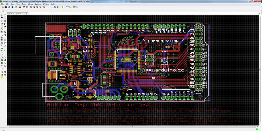
Creating the Printed Circuit Board Layout
The final step in designing a circuit in KiCad is to create the printed circuit board layout. This is where you arrange the components and their connections on a physical board. To create the PCB layout in KiCad, open the PCBnew program and import the netlist file you generated in the previous step. Then, place the components on the board and route the connections between them. KiCad has a powerful auto-router that can help you with this task, but it is often best to manually route the connections to ensure the best performance.
In conclusion, designing a circuit using KiCad involves three main steps: creating the schematic diagram, generating the netlist, and creating the printed circuit board layout. Each step is essential to ensuring a successful circuit design. With the help of KiCad’s powerful tools, anyone can design a circuit, whether they are a professional engineer or a hobbyist.
Customizing the Circuit
Editing the Schematic Diagram
One of the great benefits of using KiCad is the ability to customize your circuit design. You can modify the schematic diagram by adding, deleting, or changing components. To edit the schematic diagram, simply double-click on the component you want to modify. This will open the component properties window, where you can make changes to the component’s properties.
Customizing the PCB Layout
After designing the schematic diagram, you can customize the PCB layout. This involves placing the components on the board, routing the traces, and adding vias. KiCad offers a range of tools to help you customize the PCB layout, including a component placement tool, a trace routing tool, and a via placement tool.
To customize the PCB layout, you can use the drag-and-drop feature to move components around the board. You can also use the trace routing tool to route the traces between the components. Additionally, you can add vias to connect different layers of the board.
Adding 3D Models to the PCB
KiCad also allows you to add 3D models to your PCB design. This can be useful for visualizing the final product and identifying any potential issues with the design. To add a 3D model to your PCB design, you can import the model into KiCad and then place it on the board.
In conclusion, customizing your circuit design in KiCad is a straightforward process that involves editing the schematic diagram, customizing the PCB layout, and adding 3D models to the PCB. With KiCad’s powerful tools and features, you can create a customized circuit design that meets your specific needs.
Generating Manufacturing Files

KiCad provides a straightforward process for generating manufacturing files that can be sent to a PCB manufacturer. The process involves generating three types of files: Gerber files, drill files, and a bill of materials.
Generating Gerber Files
Gerber files are the standard format for PCB manufacturing. They contain information about the copper traces, pads, and other features of the PCB. To generate Gerber files in KiCad, go to File > Plot. In the Plot window, select the layers you want to include in the Gerber files, and choose the output directory. KiCad will generate a separate Gerber file for each layer you select.
Generating Drill Files
Drill files contain information about the holes that need to be drilled in the PCB. To generate drill files in KiCad, go to File > Plot. In the Plot window, select the Drill file option, and choose the output directory. KiCad will generate a separate drill file for each drill size used in your PCB design.
Generating Bill of Materials
A bill of materials (BOM) lists all the components used in your PCB design. It is a critical document for PCB assembly, and it helps ensure that all the necessary components are ordered and assembled correctly. To generate a BOM in KiCad, go to File > Generate Bill of Materials. KiCad will generate a CSV file containing all the components used in your PCB design.
In summary, generating manufacturing files in KiCad is a straightforward process that involves generating Gerber files, drill files, and a bill of materials. By following these steps, you can ensure that your PCB design is manufacturable and ready for assembly.
