Prototype PCB design is a crucial step in the development of electronic devices. It involves creating a working model of a printed circuit board (PCB) before mass production. This allows for testing and refinement of the design, ensuring that the final product meets the desired specifications.
There are many factors to consider when designing a prototype PCB, such as the size and shape of the board, the placement of components, and the routing of traces. It is important to choose the right materials and manufacturing processes to ensure that the prototype functions as intended. With the right design and testing process, a prototype PCB can help to identify and address any issues before mass production, saving time and money in the long run.
Overall, prototype PCB design is a crucial step in the development of electronic devices. By creating and testing a working model of a PCB, designers can ensure that the final product meets the desired specifications and functions as intended. With the right design and testing process, prototype PCBs can help to identify and address any issues before mass production, ultimately leading to a better final product.
What is Prototype PCB Design?
Prototype PCB design is the process of creating a printed circuit board (PCB) for a new product or device that is still in the development phase. A PCB is a board made of insulating material with conductive pathways etched onto it, which allows for the connection of electronic components.
Prototype PCB design is an essential step in the development of any electronic device, as it allows engineers and designers to test and refine their designs before moving to mass production. During the prototype PCB design process, engineers can identify and resolve any issues with the circuitry, layout, or components, ensuring that the final product functions as intended.
There are several key steps involved in prototype PCB design, including schematic capture, PCB layout, and fabrication. Schematic capture involves creating a visual representation of the circuit design, while PCB layout involves designing the physical layout of the board. Fabrication involves manufacturing the board itself, which can be done using a variety of techniques, including etching, milling, or printing.
Overall, prototype PCB design is an essential part of the product development process for any electronic device. By creating a functional prototype, engineers and designers can ensure that their product meets the necessary specifications and functions as intended.
Why is Prototype PCB Design Important?
Prototype PCB design is a crucial step in the process of creating a new electronic product. It allows engineers to test and validate their design before moving on to the manufacturing stage. In this section, we will explore the reasons why prototype PCB design is so important.
Minimizes Costly Mistakes
One of the main benefits of prototype PCB design is that it helps to identify and correct errors early in the design process. This can save a significant amount of time and money in the long run. Without a prototype, errors may not be discovered until the product is in the hands of the customer, which can lead to costly recalls and repairs.
Improves Design Quality
Prototype PCB design also allows engineers to fine-tune their design and make improvements before going into mass production. By testing the prototype, they can identify any areas that need improvement and make changes to optimize the product’s performance and reliability.
Speeds Up Time to Market
By catching errors early in the design process and improving the design quality, prototype PCB design can help speed up the time to market for a new product. This is especially important in today’s fast-paced business environment, where being first to market can make all the difference.
Enables Customization
Finally, prototype PCB design allows for customization of the product to meet the specific needs of the customer. By testing different configurations and designs, engineers can create a product that is tailored to the customer’s requirements.
In conclusion, prototype PCB design is a critical step in the process of creating a new electronic product. It helps to minimize errors, improve design quality, speed up time to market, and enable customization. By investing time and resources in prototype PCB design, companies can create better products that meet the needs of their customers.
The Prototype PCB Design Process

The prototype PCB design process involves several steps that must be followed carefully to ensure the successful development of a functional printed circuit board. The process begins with the design and layout of the board, followed by the fabrication of the board, and finally, the assembly of the components onto the board.
Design and Layout
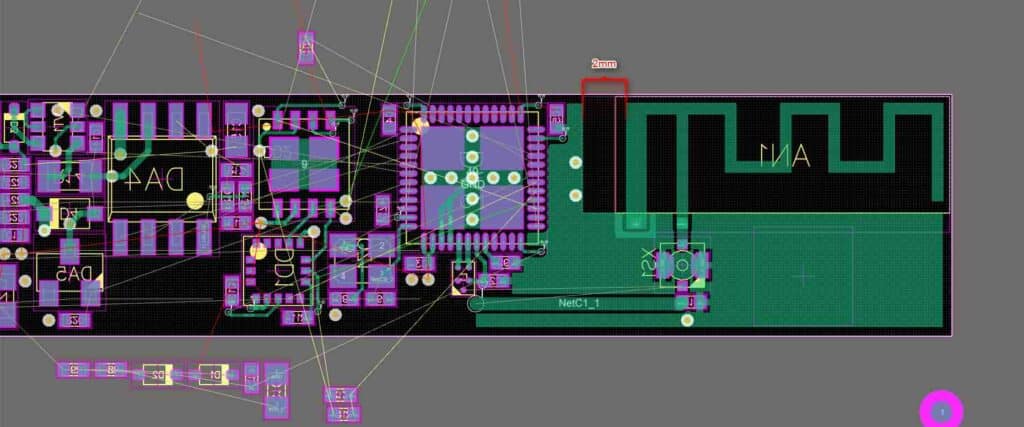
The design and layout stage is critical to the success of the prototype PCB. During this stage, the designer uses specialized software to create a schematic of the circuit and then translates it into a physical layout. The layout must take into account the size and shape of the board, the placement of components, and the routing of traces. The designer must also consider factors such as signal integrity, power distribution, and thermal management.
Fabrication
Once the design and layout are complete, the next step is to fabricate the board. This involves transferring the design onto the actual PCB substrate, which is typically made of fiberglass or another insulating material. The board is then coated with copper, and the excess copper is etched away to create the desired traces and pads.
Component Assembly
The final stage of the prototype PCB design process is the assembly of the components onto the board. This involves placing the components onto the board and soldering them in place. The assembly process must be done carefully to avoid damaging the components or the board itself.
In conclusion, the prototype PCB design process is a complex and multi-step process that requires careful planning and execution. By following the steps outlined above, designers can create functional and reliable printed circuit boards for a wide range of applications.
Designing the Schematic
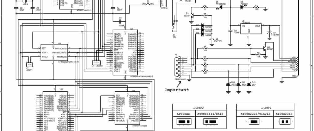
The schematic is the backbone of any PCB design. It is a graphical representation of the electrical connections and components that make up the circuit. A well-designed schematic is critical to the success of a PCB project.
When designing the schematic, it is important to keep the following tips in mind:
-
Start with a clear understanding of the project requirements: Before beginning the schematic design, it is important to have a clear understanding of the project requirements. This includes understanding the functionality of the circuit, the components needed, and the electrical specifications.
-
Organize the schematic for readability: A well-organized schematic is easier to read and understand. It is important to group related components together and to use clear, concise labels for each component.
-
Use standard symbols: Using standard symbols for components and electrical connections makes the schematic easier to read and understand. It is important to use symbols that are widely recognized in the industry.
-
Add comments and notes: Adding comments and notes to the schematic can help to explain the functionality of the circuit and can make it easier to troubleshoot any issues that arise.
-
Consider the layout: While designing the schematic, it is important to consider the layout of the PCB. Components should be placed in a logical and efficient manner, and the routing of electrical connections should be considered.
In summary, designing the schematic is a critical step in the PCB design process. By following these tips, designers can create a well-organized and easy-to-understand schematic that will lead to a successful PCB project.
Creating the Layout
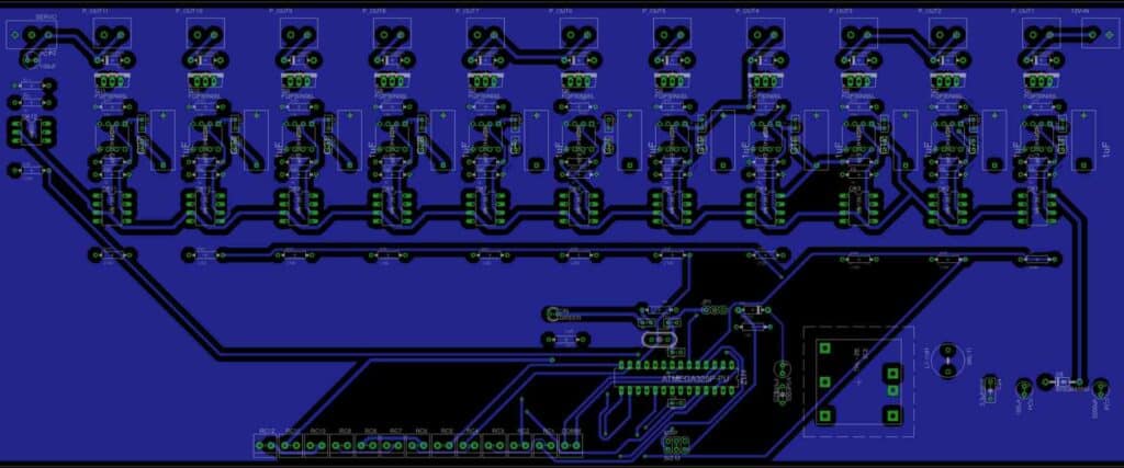
Once you have completed the schematic design, the next step is to create the layout for your prototype PCB. This involves arranging the components on the board and routing the connections between them.
When creating the layout, it is important to consider the physical dimensions of the board and the size and placement of the components. You should also take into account any specific requirements for your design, such as power and ground planes, signal integrity, and thermal management.
To simplify the process of creating the layout, you can use a PCB design software tool, such as Eagle, Altium, or KiCAD. These tools provide a range of features, including auto-routing, design rule checking, and 3D visualization, which can help you create a high-quality layout quickly and efficiently.
When designing the layout, it is important to follow best practices for PCB layout, such as:
- Placing components in a logical and organized manner
- Keeping traces as short and direct as possible
- Minimizing the number of vias and avoiding overlapping traces
- Using a ground plane to reduce noise and improve signal integrity
- Ensuring that the board is properly grounded and shielded, if necessary
By following these guidelines, you can create a layout that meets your design requirements and is optimized for performance and reliability. Once you have completed the layout, you can export the design files and send them to a PCB manufacturer for fabrication.
In summary, creating the layout for a prototype PCB involves arranging the components and routing the connections between them. By using a PCB design software tool and following best practices for layout, you can create a high-quality design that meets your requirements and is optimized for performance and reliability.
Ordering Prototype PCBs
Once you have designed your PCB layout, the next step is to order a prototype PCB. Ordering a prototype PCB is a critical step in the design process, as it allows you to test your design and make any necessary changes before moving on to the final production stage. Here are a few things to keep in mind when ordering your prototype PCB:
PCB Manufacturer
Choosing the right PCB manufacturer is crucial to ensure the quality of your prototype PCB. There are many PCB manufacturers out there, so it’s important to do your research and choose a reputable company that offers high-quality PCBs at a reasonable price. Look for reviews and testimonials from other customers to help you make an informed decision.
PCB Specifications
When ordering your prototype PCB, make sure to specify all the necessary details, such as the number of layers, board thickness, copper weight, and surface finish. You should also provide the manufacturer with your Gerber files, which contain all the necessary information about your PCB design.
Lead Time
The lead time for your prototype PCB can vary depending on the manufacturer and the complexity of your design. Make sure to check the lead time with the manufacturer before placing your order, as you may need to adjust your timeline accordingly.
Cost
The cost of your prototype PCB will depend on several factors, such as the size, complexity, and quantity of your boards. Make sure to get a quote from the manufacturer before placing your order, and consider ordering in bulk to save on costs.
Quality Control
Before shipping your prototype PCB, the manufacturer should perform a thorough quality control check to ensure that it meets your specifications. Make sure to inspect your PCB carefully upon receipt to ensure that it functions as expected.
By following these guidelines, you can ensure that your prototype PCB is of high quality and meets your design requirements.
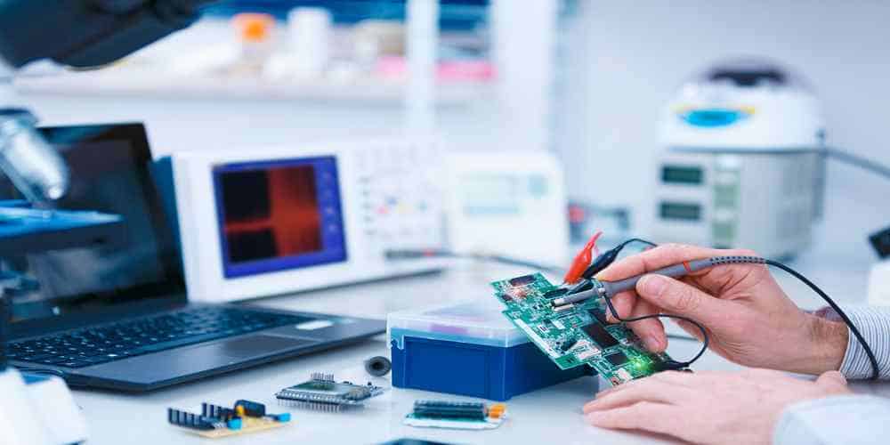
Testing the Prototype PCB
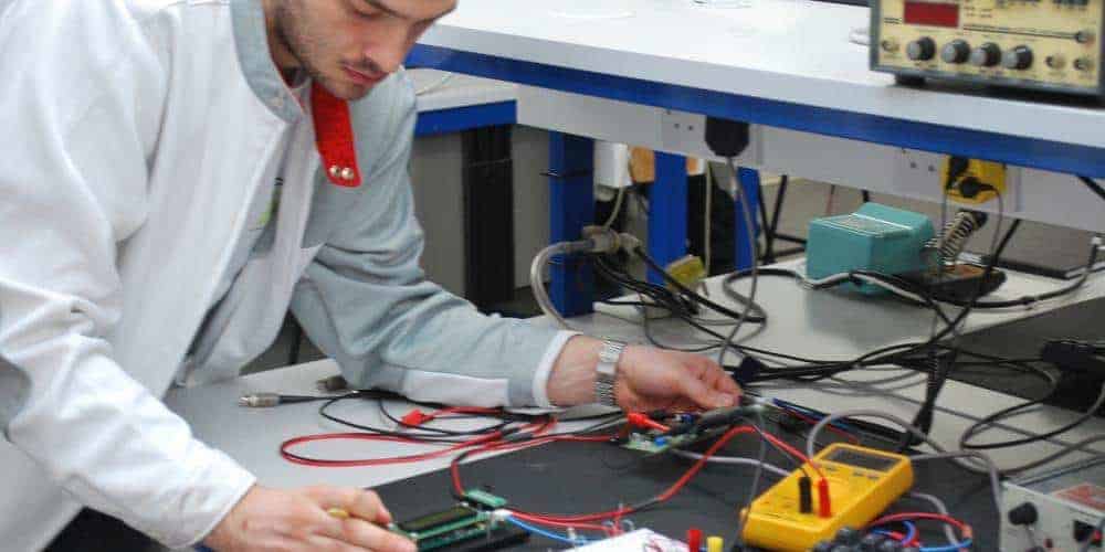
Once the prototype PCB has been designed and assembled, it is essential to test it thoroughly to ensure it meets the required specifications. The testing process involves verifying that the hardware and software work as intended and that the PCB can withstand the expected operating conditions.
Hardware Testing
Hardware testing is the process of checking the functionality of the PCB’s components and verifying that they are correctly connected. The following tests are typically performed during hardware testing:
- Visual inspection: The PCB is visually inspected to ensure that all components are correctly placed, and there are no visible defects such as solder bridges or missing components.
- Continuity testing: A multimeter is used to check the continuity of each net on the PCB to ensure that there are no open or short circuits.
- Power supply testing: The power supply is checked to ensure that the PCB is receiving the correct voltage and current.
Software Testing
Software testing is the process of verifying that the firmware or software running on the PCB works as intended. The following tests are typically performed during software testing:
- Functional testing: The software is tested to ensure that it performs the intended functions correctly.
- Performance testing: The software is tested to ensure that it meets the required performance specifications, such as speed and accuracy.
- Stress testing: The software is tested under extreme conditions to ensure that it can handle unexpected inputs or events.
Environmental Testing
Environmental testing is the process of verifying that the PCB can withstand the expected operating conditions. The following tests are typically performed during environmental testing:
- Temperature testing: The PCB is tested at various temperatures to ensure that it can operate within the specified temperature range.
- Vibration testing: The PCB is subjected to vibration to ensure that it can withstand the expected vibration levels.
- Humidity testing: The PCB is tested at various humidity levels to ensure that it can operate in humid environments.
In conclusion, testing the prototype PCB is a critical step in the design process. It ensures that the PCB meets the required specifications and can operate under the expected operating conditions.
Common Mistakes in Prototype PCB Design
When designing a prototype PCB, there are several common mistakes that engineers and designers make. These mistakes can lead to wasted time, money, and resources. Here are some of the most common mistakes to avoid:
1. Not Considering the Physical Size and Shape of Components
One of the most common mistakes in prototype PCB design is not considering the physical size and shape of components. It’s important to ensure that all components fit on the board and that there is enough space between them to prevent short circuits. It’s also important to consider the height of the components to ensure that they don’t interfere with other components or the enclosure.
2. Not Following Design Rules and Guidelines
Another common mistake is not following design rules and guidelines. These rules and guidelines are in place to ensure that the PCB functions properly and is manufacturable. Not following these rules can lead to errors in the design and make it difficult or impossible to manufacture the PCB.
3. Not Testing the Design Before Ordering the PCB
It’s important to test the design before ordering the PCB. This can help identify any errors or issues in the design before it’s too late. Prototyping the design can also help identify any issues with the physical layout of the components and ensure that everything fits on the board.
4. Not Considering the Power Requirements
Another common mistake is not considering the power requirements of the PCB. It’s important to ensure that the PCB can handle the required voltage and current without overheating or causing damage to the components.
5. Not Considering the Environmental Conditions
Finally, not considering the environmental conditions can lead to issues with the PCB. It’s important to consider factors such as temperature, humidity, and vibration when designing the PCB to ensure that it can function properly in its intended environment.
By avoiding these common mistakes, engineers and designers can create prototype PCBs that are functional, manufacturable, and reliable.
Best Practices for Prototype PCB Design
When it comes to prototype PCB design, there are several best practices that can help ensure a successful outcome. Here are a few key tips to keep in mind:
-
Start with a clear design plan: Before you begin designing your PCB, take the time to create a clear plan that outlines your requirements, constraints, and goals. This will help you stay organized and focused throughout the design process.
-
Use design software: There are many design software options available for PCB design. Using software can help you create more accurate designs and make changes more easily.
-
Follow design guidelines: Most PCB manufacturers will provide design guidelines that you should follow to ensure your design meets their requirements. Make sure to review and follow these guidelines to avoid any issues during the manufacturing process.
-
Consider the manufacturing process: When designing your PCB, keep in mind the manufacturing process that will be used to produce it. For example, if you plan to use surface mount technology, make sure to design your board with the appropriate pad sizes and spacing.
-
Test and iterate: Once you have a prototype PCB design, it’s important to test it thoroughly to identify any issues or areas for improvement. Iterate on your design as needed to optimize its performance.
By following these best practices, you can increase the likelihood of a successful prototype PCB design.
Conclusion
In conclusion, prototype PCB design is a crucial step in the development of electronic products. It allows engineers to test and refine their designs before moving on to the production stage. Through the use of various design software and tools, designers can create efficient and reliable PCBs that meet their specific requirements.
During the design process, it is important to consider factors such as component placement, routing, and signal integrity. These factors can significantly impact the performance of the final product. To ensure a successful design, it is recommended to follow industry standards and guidelines.
Prototyping can also help identify potential issues and improve the overall quality of the design. By testing and iterating, designers can refine their designs and ensure that they meet the necessary specifications. This can save time and money in the long run by avoiding costly mistakes and reducing the need for redesigns.
Overall, prototype PCB design is a critical step in the development of electronic products. By following best practices and utilizing the appropriate tools and techniques, designers can create high-quality PCBs that meet their specific needs.
