The ATmega328P is a popular microcontroller chip that is widely used in various electronic projects. It is commonly found in Arduino boards and is known for its versatility and ease of use. However, designing a printed circuit board (PCB) layout for the ATmega328P can be a challenging task.
The PCB layout is a crucial aspect of any electronic design, as it determines the physical arrangement of the components on the board. A well-designed PCB layout can improve the performance and reliability of the circuit, while a poorly designed layout can lead to various issues such as noise, interference, and signal loss. In the case of the ATmega328P, the layout must be carefully planned to ensure that the various pins and components are properly connected and arranged. This article will provide an overview of the important considerations when designing a PCB layout for the ATmega328P, including pin mapping, power supply, and signal routing.
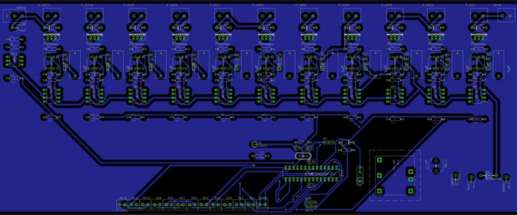
ATmega328P PCB Layout Basics
When designing a PCB layout for the ATmega328P microcontroller, it is important to keep in mind the basic principles of schematic design, component placement, and routing. Following these principles will help ensure the reliability and functionality of the final product.
Schematic Design
The first step in designing a PCB layout for the ATmega328P is to create a schematic diagram. This diagram should include all of the necessary components, such as resistors, capacitors, and voltage regulators, as well as the ATmega328P microcontroller itself.
When creating the schematic, it is important to keep the layout clean and organized. Group related components together and use consistent labeling to make it easier to understand and modify the design later on.
Component Placement
Once the schematic is complete, the next step is to place the components on the PCB layout. When placing components, it is important to consider factors such as signal integrity, thermal management, and accessibility for testing and debugging.
Group components together based on their function and keep them as close together as possible. This will help reduce the length of signal traces and minimize the risk of electromagnetic interference.
Routing
After the components are placed, the next step is to route the traces between them. When routing, it is important to consider the signal requirements of each component and use appropriate trace widths and spacing.
It is also important to keep the traces as short and direct as possible to minimize signal degradation and interference. Use ground planes and power planes to provide a low-impedance return path for signals and reduce the risk of noise and interference.
By following these basic principles of schematic design, component placement, and routing, designers can create reliable and functional PCB layouts for the ATmega328P microcontroller.
PCB Design Considerations

When designing a printed circuit board (PCB) for the Atmega328P microcontroller, there are several important considerations to keep in mind. These include power supply design, clock circuit design, signal integrity, and electromagnetic interference (EMI) considerations.
Power Supply Design
The Atmega328P requires a stable and clean power supply in order to function properly. When designing the power supply for the PCB, it is important to consider factors such as voltage regulation, noise filtering, and decoupling capacitors. A good power supply design will ensure that the microcontroller receives a stable and clean supply of power, which will improve its overall performance and reliability.
Clock Circuit Design
The Atmega328P relies on an accurate clock signal in order to execute instructions at the correct time. When designing the clock circuit for the PCB, it is important to consider factors such as clock frequency, crystal selection, and PCB layout. A well-designed clock circuit will ensure that the microcontroller operates at the correct frequency and with minimal jitter.
Signal Integrity
Signal integrity is an important consideration when designing any PCB, and it is especially important when working with high-speed microcontrollers like the Atmega328P. Factors that can affect signal integrity include trace length, impedance matching, and noise. By carefully designing the PCB layout and implementing best practices for signal integrity, it is possible to ensure that the microcontroller operates reliably and without errors.
EMI Considerations
EMI, or electromagnetic interference, can be a significant problem in PCB design. EMI can cause noise and interference in the microcontroller’s signals, leading to errors and reduced performance. When designing a PCB for the Atmega328P, it is important to consider factors such as grounding, shielding, and component placement in order to minimize EMI and ensure reliable operation.
In summary, designing a PCB for the Atmega328P requires careful consideration of factors such as power supply design, clock circuit design, signal integrity, and EMI considerations. By paying close attention to these factors and implementing best practices in PCB design, it is possible to create a reliable and high-performance PCB for the Atmega328P microcontroller.
PCB Design Tools
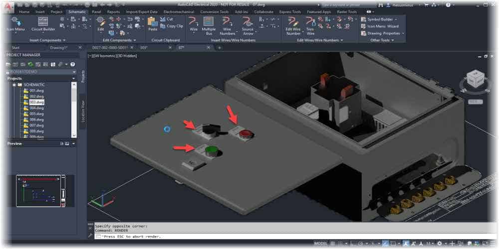
When designing a PCB layout for the ATmega328P microcontroller, it is important to choose the right PCB design tool. Here are three popular options:
Eagle
Eagle is a widely-used PCB design software that offers a user-friendly interface and a large library of components. It has a free version with certain limitations and a paid version with more features. Eagle is known for its compatibility with a wide range of operating systems, including Windows, Mac, and Linux.
Altium Designer
Altium Designer is a professional-grade PCB design software that is known for its advanced features and high-quality output. It offers a comprehensive library of components and a powerful design engine. Altium Designer is a popular choice among professional PCB designers, but it comes with a higher price tag than other options.
KiCAD
KiCAD is a free and open-source PCB design software that is gaining popularity among hobbyists and professionals alike. It offers a user-friendly interface and a wide range of features, including schematic capture, PCB layout, and 3D visualization. KiCAD is compatible with Windows, Mac, and Linux.
In conclusion, choosing the right PCB design tool is crucial for creating a successful ATmega328P PCB layout. Each of these three options offers unique benefits and drawbacks, so it is important to carefully consider your needs and budget before making a decision.
PCB Manufacturing and Assembly
Gerber Files Generation
Before manufacturing the PCB, the Gerber files must be generated. Gerber files are the industry standard file format used to convey PCB design information to PCB manufacturers. They include all the necessary information about the PCB design, such as the location of components, copper traces, and drill holes.
PCB Fabrication Process
Once the Gerber files are generated, the PCB fabrication process can begin. This process involves several steps, including the application of a photosensitive layer to the copper-clad board, exposure to UV light, and the removal of the unexposed photosensitive layer. After this, the board is etched to remove the unwanted copper and drilled to create the necessary holes for components.
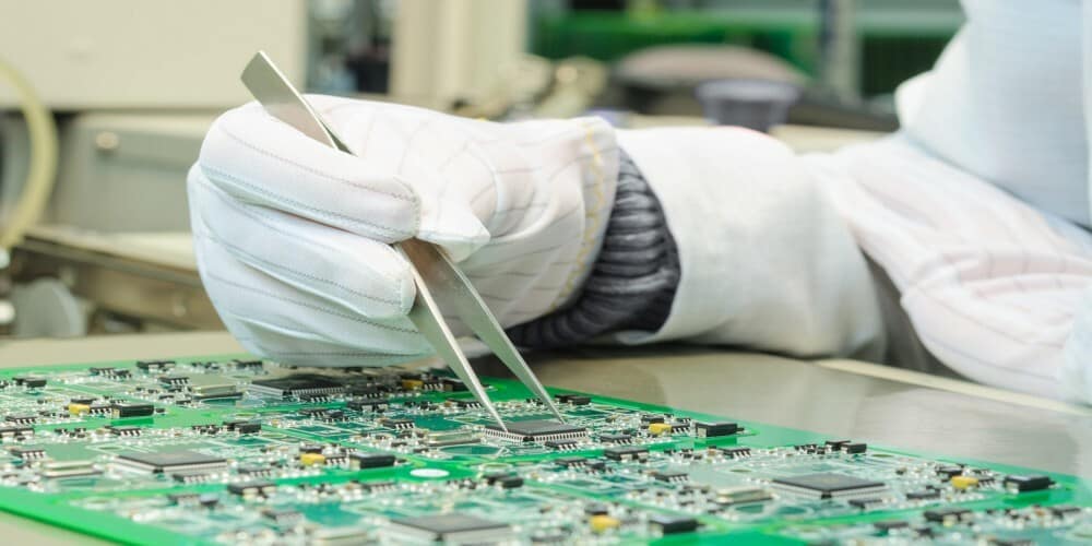
PCB Assembly Process
After the PCB is fabricated, the next step is to assemble the components onto the board. This process involves placing the components on the board and soldering them in place. There are two main methods of PCB assembly: through-hole and surface mount.
Through-hole assembly involves inserting the leads of components through holes drilled into the board and then soldering them in place. Surface mount assembly, on the other hand, involves soldering the components directly to the surface of the board.
In both cases, the soldering process can be done manually or with the use of automated equipment. Once the components are soldered in place, the PCB is inspected for any defects or issues before being shipped out.
Overall, the PCB manufacturing and assembly process is a crucial step in bringing a circuit design to life. By following best practices and ensuring quality control throughout the process, a reliable and functional PCB can be produced.
