PCB design is an essential aspect of creating electronic devices, including those that utilize the popular Arduino platform. Printed circuit boards, or PCBs, are used to connect the various components of a device, providing a more efficient and reliable method of communication than traditional wiring. Proper PCB design is crucial for ensuring that a device functions correctly and safely.
When designing a PCB for an Arduino project, there are a few key factors to consider. These include the size and shape of the board, the placement of components, and the routing of traces. It is important to ensure that the board is appropriately sized for the project and that components are placed in a logical and efficient manner. Additionally, the routing of traces is critical for minimizing interference and ensuring that the device functions correctly. By taking these factors into account, designers can create PCBs that are both functional and aesthetically pleasing.
Basics of PCB Design
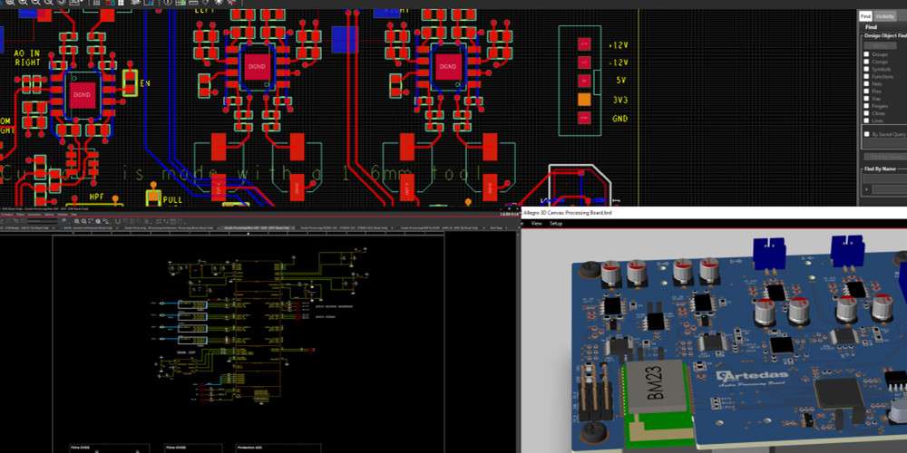
When designing a printed circuit board (PCB) for an Arduino project, there are two main stages to consider: schematic design and PCB layout design.
Schematic Design
The schematic design is the first step in PCB design. It involves creating a graphical representation of the circuit that you want to build. This representation is made up of symbols that represent the components of the circuit, and lines that connect these components together.
When designing the schematic, it is important to ensure that all of the components are connected correctly and that there are no errors. This will help to avoid any problems during the PCB layout design stage.
PCB Layout Design
The PCB layout design is the second stage in PCB design. It involves taking the schematic that you have created and turning it into a physical circuit board. This involves placing the components onto the board and routing the connections between them.
When designing the PCB layout, it is important to consider factors such as the size of the board, the location of the components, and the routing of the connections. It is also important to ensure that the board is designed in a way that is easy to manufacture.
Overall, the schematic design and PCB layout design are two important stages in PCB design. By taking the time to design a well thought out schematic and PCB layout, you can ensure that your Arduino project will work correctly and be easy to manufacture.
Arduino Board Design

Choosing an Arduino Board
When it comes to choosing an Arduino board for your project, there are a few things to consider. First, think about the size of your project and the number of inputs and outputs you will need. If you have a small project with only a few sensors or actuators, a smaller board like the Arduino Nano or Micro might be sufficient. However, if you have a larger project with many inputs and outputs, you might want to consider a board like the Arduino Mega or Due.
Another consideration is the type of microcontroller used on the board. For example, the Arduino Uno uses the ATmega328P microcontroller, while the Arduino Due uses the SAM3X8E microcontroller. Different microcontrollers have different capabilities and specifications, so choose the one that best fits your project’s needs.
Designing Custom Arduino Board
If you can’t find an Arduino board that meets your project’s requirements, you can design and build your own custom board. This allows you to tailor the board to your specific needs and can save you space and money.
To design a custom Arduino board, you will need to choose a microcontroller and build the necessary circuitry around it. You can use the Arduino schematic and reference designs as a starting point, but you will need to modify them to fit your specific needs.
When designing your board, be sure to follow best practices for PCB design, such as keeping traces short and avoiding sharp corners. You should also test your board thoroughly before using it in your project to ensure that it works as intended.
In summary, choosing the right Arduino board for your project is important, and if you can’t find one that meets your needs, designing your own custom board can be a great option. By considering factors like size, inputs and outputs, and microcontroller type, you can select or design a board that will work well for your project.
Designing PCB for Arduino
When designing a PCB for Arduino, there are a few key steps to follow to ensure a successful project. These steps include selecting the appropriate components, designing the schematic diagram, and designing the PCB layout diagram.
Components Selection
The first step in designing a PCB for Arduino is selecting the appropriate components. This includes choosing the right microcontroller, voltage regulator, and any other necessary components such as resistors, capacitors, and LEDs. It is important to select components that are compatible with the Arduino board and meet the project’s requirements.
Designing Schematic Diagram
Once the components have been selected, the next step is to design the schematic diagram. This diagram shows the connections between the components and how they are connected to the Arduino board. It is important to ensure that the connections are correct and that all components are properly connected.
Designing PCB Layout Diagram
After the schematic diagram has been designed, the next step is to design the PCB layout diagram. This diagram shows the physical layout of the components on the PCB. It is important to ensure that the layout is optimized for the project’s requirements and that there is enough space for all components.
When designing the PCB layout diagram, it is important to consider factors such as the size of the board, the number of components, and the placement of connectors and other components. It is also important to ensure that the board is designed to be easy to manufacture and assemble.
In conclusion, designing a PCB for Arduino requires careful consideration of the components, schematic diagram, and PCB layout diagram. By following these steps, it is possible to create a successful PCB design that meets the project’s requirements.
PCB Fabrication and Assembly
PCB Fabrication Process
PCB fabrication is the process of creating a printed circuit board (PCB) from a design file. The process involves several steps, including designing the PCB layout, printing the design onto a copper-clad board, etching away the unwanted copper, and drilling holes for components.
The first step in the PCB fabrication process is to create a design file using a PCB design software. The design file contains all the information needed to create the PCB, including the dimensions, component placement, and routing information.
Once the design file is ready, it is printed onto a copper-clad board using a special printer. The printer uses a special ink that is resistant to acid, which is used to etch away the unwanted copper.
After the design is printed onto the board, it is placed in an etching bath, which removes the unwanted copper. The etching process leaves behind the copper traces and pads needed to connect the components.
Finally, the board is drilled to create holes for the components. The holes are then plated with copper to create a strong connection between the components and the traces.
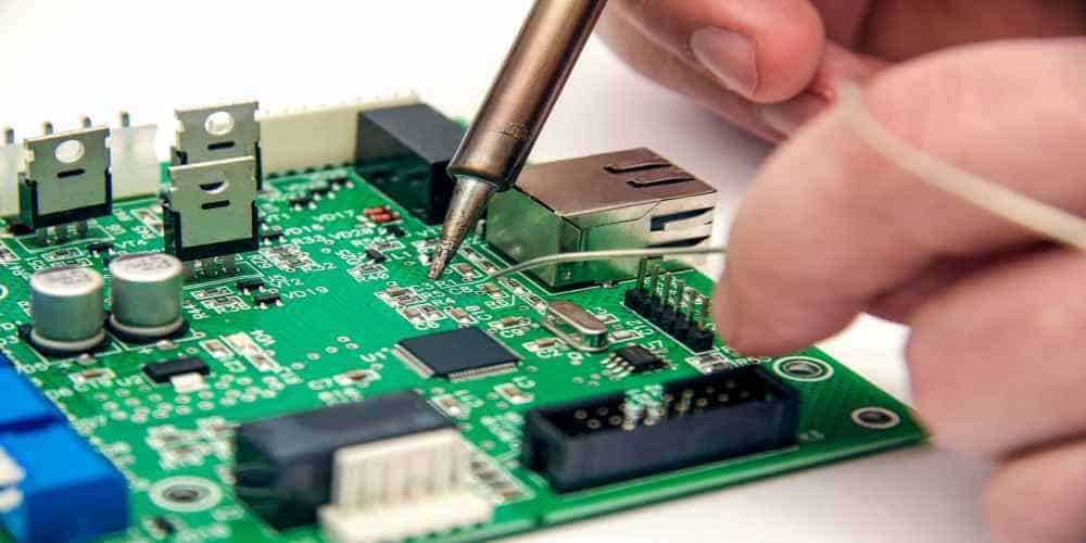
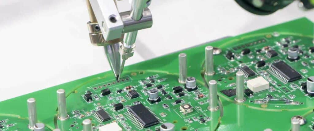
PCB Assembly Process
PCB assembly is the process of attaching components to a printed circuit board (PCB). The process involves several steps, including placing the components on the board, soldering them in place, and testing the board to ensure it works correctly.
The first step in the PCB assembly process is to place the components on the board. This is done using a pick-and-place machine, which picks up the components and places them in the correct location on the board.
Once the components are in place, they are soldered onto the board. This is done using a soldering machine, which melts the solder and creates a strong bond between the components and the board.
After the board is soldered, it is tested to ensure it works correctly. This is done using a variety of tests, including visual inspection, electrical testing, and functional testing.
Overall, the PCB fabrication and assembly process is a complex but essential part of creating an Arduino project. By following these steps, you can create a high-quality PCB that will work reliably and efficiently.
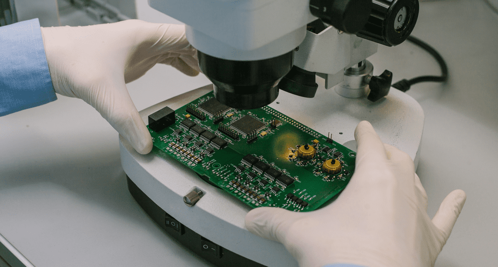
Testing and Troubleshooting
Testing PCB Design
Once the PCB design has been completed, it is essential to test it to ensure that it is functioning correctly. There are several ways to test a PCB design. One of the simplest ways to test a PCB is by using a multimeter. A multimeter can be used to check the continuity of the circuit, the voltage levels, and the resistance of the components used in the circuit.
Another way to test a PCB design is by using an oscilloscope. An oscilloscope can be used to check the waveform of the signals in the circuit. This is particularly useful when testing analog circuits.
Troubleshooting PCB Design
Even with careful design and testing, it is not uncommon for issues to arise with the PCB design. When troubleshooting a PCB design, it is important to have a systematic approach to the process.
The first step in troubleshooting a PCB design is to identify the problem. This can be done by checking the circuit for continuity, voltage levels, and resistance using a multimeter or an oscilloscope. Once the problem has been identified, the next step is to isolate the faulty component or components.
If the faulty component cannot be easily identified, it may be necessary to use a logic analyzer. A logic analyzer can be used to monitor the signals in the circuit and identify where the problem is occurring.
In some cases, the problem may be caused by a design flaw. In such cases, it may be necessary to go back to the design stage and make the necessary changes to the PCB design.
Overall, testing and troubleshooting are essential parts of the PCB design process. By testing the design and having a systematic approach to troubleshooting issues, it is possible to ensure that the PCB design is functioning correctly and to identify and fix any issues that may arise.
