Designing custom PCBs can be an intimidating task for beginners, but it doesn’t have to be. With the right tools and knowledge, anyone can create a custom PCB that meets their specific needs. Whether you’re a hobbyist looking to build a custom electronic device or a professional engineer working on a new product, designing a custom PCB can save you time, money, and headaches in the long run.
One of the first steps in designing a custom PCB is to choose the right software. There are many different PCB design software options available, each with its own strengths and weaknesses. Some popular options include Eagle, Altium, and KiCAD. Once you’ve chosen your software, it’s important to familiarize yourself with its features and capabilities. This will help you make the most of the software and design a PCB that meets your specific needs.
Designing a Custom PCB
Defining the PCB Design Process
Designing a custom PCB requires a well-defined process to ensure that the final product meets the desired specifications. The process typically involves several steps, including schematic capture, layout design, design rule check, and Gerber file generation. Defining the process beforehand can help to streamline the design process and ensure that the final product meets the desired specifications.
Choosing the Right Software
Choosing the right software is critical to the success of any PCB design project. Several software options are available, each with its own set of features and capabilities. Some popular software options for PCB design include Altium Designer, Eagle PCB, and KiCAD. It is important to select software that meets the specific needs of the project and is compatible with the hardware and software used in the design process.
Schematic Capture
Schematic capture is the process of creating a graphical representation of the circuit that will be implemented on the PCB. This step involves adding components to the schematic and connecting them with wires or other electrical connections. The schematic is a critical part of the design process as it provides a clear understanding of the circuit and its functionality.
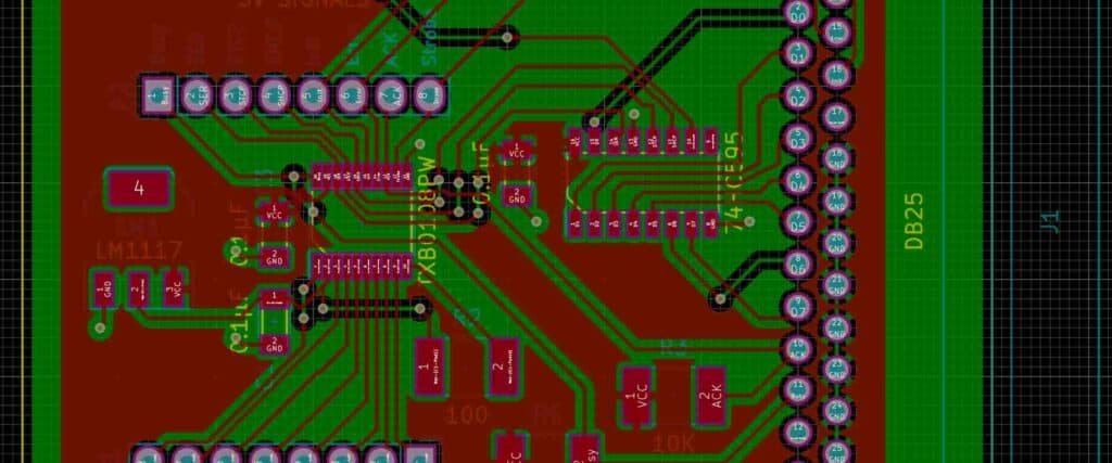
Layout Design
Layout design is the process of arranging the components and electrical connections on the PCB. The layout design should take into account the physical constraints of the PCB and the electrical requirements of the circuit. The layout should be optimized for signal integrity, thermal management, and manufacturability.
Design Rule Check
The design rule check is a critical step in the PCB design process. This step involves verifying that the layout design meets the design rules and guidelines specified by the manufacturer. The design rule check ensures that the final product is manufacturable and meets the desired specifications.
Gerber File Generation
The Gerber file generation is the final step in the PCB design process. This step involves converting the layout design into a set of files that can be used by the manufacturer to produce the PCB. The Gerber files include information about the electrical connections, component placement, and other design details.
In conclusion, designing a custom PCB requires a well-defined process, the right software, and attention to detail. By following the steps outlined above, you can create a high-quality PCB that meets the desired specifications.
Prototyping and Testing
Prototyping Tools and Techniques
When designing a custom PCB, prototyping is a crucial step to ensure that the design is functional and meets the required specifications. Prototyping can be done using various tools and techniques, including breadboarding, perfboarding, and PCB prototyping machines.
Breadboarding involves using a breadboard to connect electronic components together without the need for soldering. This technique is useful for testing and experimenting with different circuit configurations before committing to a final design.
Perfboarding, on the other hand, involves using a perforated board to mount electronic components and create a circuit. This technique is useful for creating small and simple designs that do not require a custom PCB.
PCB prototyping machines, such as CNC mills and laser cutters, can be used to create custom PCBs quickly and accurately. These machines use computer-aided design (CAD) software to generate the PCB layout and then cut the copper traces and drill the holes required for the components.
Testing and Verification
Once the prototype is built, it is important to test and verify its functionality and performance. This involves using various testing methods, including functional testing, electrical testing, and environmental testing.
Functional testing involves testing the prototype’s functionality by verifying that it performs the intended task correctly. This can be done using software simulations or by physically testing the prototype.
Electrical testing involves using a multimeter or oscilloscope to measure the electrical characteristics of the prototype, such as voltage, current, and frequency. This helps to identify any issues with the circuit design or component selection.
Environmental testing involves subjecting the prototype to different environmental conditions, such as temperature, humidity, and vibration, to ensure that it can withstand the conditions it will be exposed to in its intended application.
By using the right prototyping tools and techniques and performing thorough testing and verification, designers can ensure that their custom PCBs are functional, reliable, and meet the required specifications.
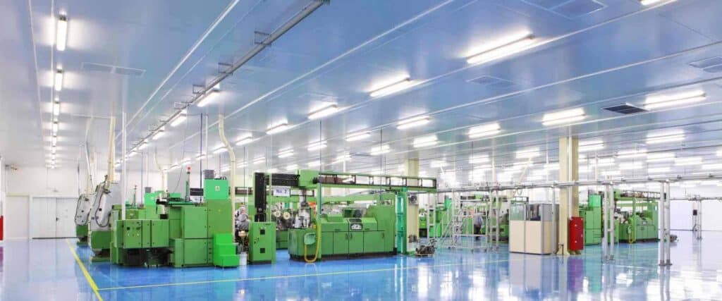
Manufacturing and Assembly

Choosing the Right Manufacturer
Choosing the right manufacturer is crucial for the success of your PCB project. You need to find a manufacturer that can meet your requirements, budget, and timeline. Here are some factors to consider when selecting a PCB manufacturer:
- Experience: Look for a manufacturer with years of experience and a proven track record of delivering high-quality PCBs.
- Capabilities: Make sure the manufacturer has the capabilities to produce the type of PCB you need. For example, if you need a multilayer PCB, make sure the manufacturer has experience with multilayer PCBs.
- Quality: Quality is paramount when it comes to PCBs. Look for a manufacturer that has a robust quality control process in place.
- Price: Price is always a consideration. Get quotes from multiple manufacturers and compare them to find the best value for your money.
- Lead Time: Consider the manufacturer’s lead time. Can they deliver the PCBs within your timeline?
Preparing for Manufacturing
Before you send your design files to the manufacturer, you need to make sure they are ready for manufacturing. Here are some steps to follow:
- Design Rule Check (DRC): Run a DRC to check for errors and make sure your design meets the manufacturer’s requirements.
- Panelization: Panelize your design to make the most efficient use of the PCB material and reduce manufacturing costs.
- Gerber Files: Generate the Gerber files and make sure they are error-free.
- Bill of Materials (BOM): Create a BOM that includes all the components needed for the PCB.
- Assembly Drawings: Create assembly drawings that show the placement of the components on the PCB.
Assembly and Testing
Once the manufacturer has produced the PCBs, it’s time for assembly and testing. Here are some steps to follow:
- Solder Paste Application: Apply solder paste to the PCB using a stencil.
- Component Placement: Place the components on the PCB using pick-and-place machines.
- Reflow Soldering: Reflow solder the components to the PCB using a reflow oven.
- Testing: Test the PCB to make sure it meets your specifications.
In conclusion, choosing the right manufacturer, preparing for manufacturing, and assembly and testing are critical steps in the PCB design process. By following these steps, you can ensure that your PCB project is a success.
Conclusion
In conclusion, designing custom PCBs can be a challenging task, but it is also a rewarding one. By following the steps outlined in this article, you can create a custom PCB that meets your specific needs and requirements.
It is important to keep in mind that designing a custom PCB requires a certain level of expertise and knowledge. If you are new to PCB design, it may be helpful to work with an experienced designer or to take a course in PCB design.
When designing your PCB, it is important to consider factors such as the size of the board, the number of components, and the power requirements. You should also consider the type of circuit you are designing and the environment in which it will be used.
By using the right tools and techniques, you can create a custom PCB that is reliable, efficient, and cost-effective. Whether you are designing a PCB for a hobby project or for a commercial application, taking the time to design it properly can save you time and money in the long run.
Overall, designing custom PCBs is an exciting and rewarding process that requires patience, attention to detail, and a willingness to learn. With the right tools and techniques, anyone can create a custom PCB that meets their specific needs and requirements.
