PCB 3D design is an essential aspect of modern electronics manufacturing. With the increasing demand for smaller and more complex electronic devices, PCB designers are required to create intricate and compact circuit boards that can accommodate numerous components. 3D design software has become an indispensable tool for PCB designers, allowing them to create virtual models of their designs before they are fabricated.
One of the primary benefits of using 3D design software for PCB design is the ability to detect and resolve potential issues before the manufacturing process. With 3D modeling, designers can simulate the assembly of their PCBs and identify any potential problems that may arise during the manufacturing process. This allows designers to make necessary modifications to their designs, reducing the risk of errors and improving the efficiency of the manufacturing process.
Another advantage of using 3D design software for PCB design is the ability to create more complex designs. With the use of 3D modeling, designers can create intricate designs with multiple layers and components, resulting in smaller and more efficient circuit boards. This not only improves the functionality of the device but also reduces the overall size, making it more portable and user-friendly.
Benefits of PCB 3D Design
PCB 3D design is a powerful tool that has revolutionized the way electronic devices are designed and manufactured. This section will explore some of the benefits of using PCB 3D design software.
Improved Visualization
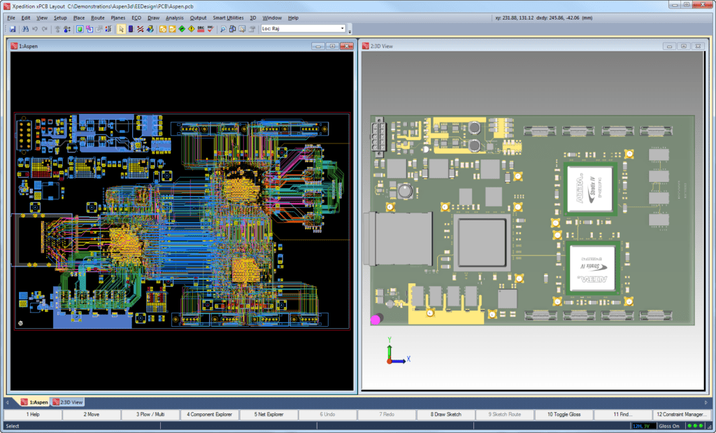
One of the most significant benefits of PCB 3D design is the ability to visualize the final product in 3D. This feature enables designers to identify and correct potential design issues before the PCB goes into production. With 3D visualization, designers can view the PCB from all angles, identify potential design flaws, and make necessary changes to the design.
Reduced Design Time
PCB 3D design software enables designers to create and modify designs quickly and easily. With 3D modeling, designers can make changes to the design in real-time, reducing the time it takes to complete the design. Additionally, designers can use pre-built libraries of components to speed up the design process further.
Enhanced Design Accuracy
PCB 3D design software provides a high level of accuracy in the design process. With 3D modeling, designers can ensure that all components are correctly placed and that there is enough space for the components to fit on the PCB. Additionally, 3D modeling allows designers to simulate the performance of the PCB before it goes into production, ensuring that the design meets all the necessary specifications.
In conclusion, PCB 3D design offers several benefits that make it an essential tool for electronic device designers. With improved visualization, reduced design time, and enhanced design accuracy, PCB 3D design software is an indispensable tool for anyone involved in the design and manufacture of electronic devices.
PCB 3D Design Tools

Overview of Available Tools
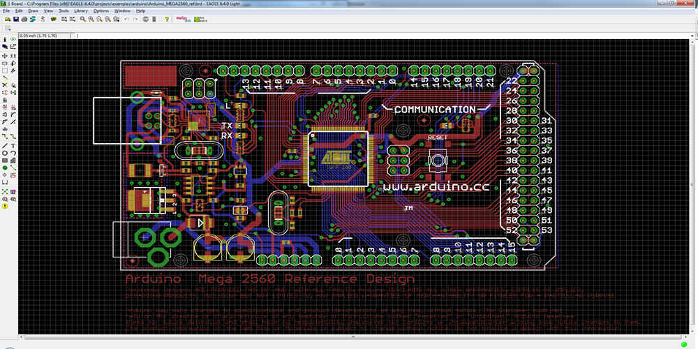
PCB 3D design tools are essential for creating accurate and effective printed circuit board designs. There are several tools available in the market that can help engineers and designers create 3D models of PCBs.
Some popular PCB 3D design tools are:
- Altium Designer
- Eagle PCB Design
- KiCAD
- Proteus PCB Design
- Cadence Allegro PCB Designer
- OrCAD PCB Designer
Each of these tools has its own unique features and capabilities that make them suitable for different applications.
Comparison of Popular Tools
Here is a brief comparison of some of the most popular PCB 3D design tools:
| Tool Name | Price | Supported Platforms | Key Features |
|---|---|---|---|
| Altium Designer | Paid | Windows | 3D modeling, schematic capture, library management |
| Eagle PCB Design | Paid | Windows, Mac, Linux | Schematic capture, layout editor, autorouter |
| KiCAD | Free | Windows, Mac, Linux | Schematic capture, PCB layout, 3D viewer |
| Proteus PCB Design | Paid | Windows | Schematic capture, PCB layout, simulation |
| Cadence Allegro PCB Designer | Paid | Windows | Schematic capture, PCB layout, 3D modeling |
| OrCAD PCB Designer | Paid | Windows | Schematic capture, PCB layout, 3D modeling, simulation |
When choosing a PCB 3D design tool, it’s important to consider factors such as price, platform compatibility, and the specific features required for the project. It’s also a good idea to read reviews and get feedback from other users to ensure that the tool is reliable and effective.
In conclusion, PCB 3D design tools are an essential part of the design process for engineers and designers. By choosing the right tool for the job, they can create accurate and effective PCB designs that meet the needs of their clients and customers.
Design Considerations
When it comes to designing a PCB in 3D, there are several important considerations that must be taken into account to ensure a successful design. These considerations include component placement, thermal management, and signal integrity.
Component Placement
One of the most critical aspects of PCB design is component placement. The placement of components on the board can have a significant impact on the performance of the circuit and the overall functionality of the device. When designing a PCB in 3D, it is important to consider the physical dimensions of the components and their placement on the board.
To ensure proper component placement, it is important to consider the following factors:
- The size and shape of the components
- The location of the components on the board
- The orientation of the components
- The spacing between the components
Thermal Management
Thermal management is another important consideration when designing a PCB in 3D. The heat generated by the components on the board can have a significant impact on the performance and reliability of the circuit. To prevent overheating and ensure proper thermal management, it is important to consider the following factors:
- The placement of components on the board
- The use of heat sinks and other cooling mechanisms
- The design of the board itself to promote airflow
Signal Integrity
Signal integrity is also a critical consideration when designing a PCB in 3D. The routing of signals on the board can have a significant impact on the performance and reliability of the circuit. To ensure proper signal integrity, it is important to consider the following factors:
- The placement of components on the board
- The routing of signals on the board
- The use of shielding and other techniques to reduce noise and interference
Overall, designing a PCB in 3D requires careful consideration of component placement, thermal management, and signal integrity. By taking these factors into account, designers can create circuits that are reliable, efficient, and effective.
PCB 3D Printing
Overview of PCB 3D Printing
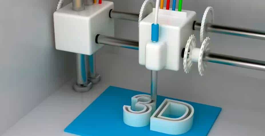
PCB 3D Printing is a process of creating three-dimensional printed circuit boards that can be used in various electronic devices. It is a relatively new technology that has gained popularity in recent years due to its ability to create complex and intricate designs.
The process involves using a 3D printer to print the circuit board design layer by layer, using conductive ink. The printer can print both the conductive and non-conductive layers, which means that it can create complex designs with ease.
Advantages of PCB 3D Printing
PCB 3D Printing has several advantages over traditional PCB manufacturing methods. Some of these advantages include:
- Faster turnaround time: PCB 3D Printing can be completed in a matter of hours, whereas traditional PCB manufacturing can take days or even weeks.
- Lower cost: PCB 3D Printing is generally cheaper than traditional PCB manufacturing, as it requires less material and labor.
- Greater design flexibility: PCB 3D Printing allows for more intricate and complex designs that are not possible with traditional PCB manufacturing methods.
- Reduced waste: PCB 3D Printing produces less waste than traditional PCB manufacturing, as it uses only the exact amount of material needed for the design.
Limitations of PCB 3D Printing
Despite its advantages, PCB 3D Printing also has some limitations. Some of these limitations include:
- Limited material options: PCB 3D Printing currently only supports a limited range of materials, which can limit its use in certain applications.
- Lower quality: The quality of the printed circuit boards may be lower than that of traditional PCBs, which can affect the performance of the electronic device.
- Size limitations: PCB 3D Printing is currently limited in terms of the size of the circuit boards that can be printed.
In conclusion, PCB 3D Printing is a promising technology that has several advantages over traditional PCB manufacturing methods. However, it also has some limitations that need to be considered before deciding whether to use it for a particular application.
