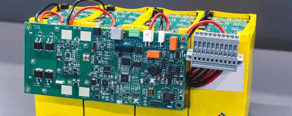
PCB circuit design is an essential aspect of modern electronics. It involves creating a printed circuit board (PCB) that connects electronic components and provides a path for electricity to flow. PCB circuit design is used in a wide range of applications, from consumer electronics to aerospace and defense systems.
In recent years, the availability of online tools and resources has made PCB circuit design more accessible than ever before. Online platforms offer a range of design tools and services, allowing engineers and hobbyists to create custom PCBs quickly and easily. These tools can be used to design circuits from scratch or to modify existing designs, making it easier to create custom solutions for specific applications. Additionally, online communities and forums provide a space for designers to share knowledge, ask questions, and collaborate on projects.
Benefits of PCB Circuit Design Online
PCB circuit design is an essential part of the electronics industry, and it has become increasingly important with the rise of the Internet. Online PCB circuit design has become more popular in recent years, and it offers several benefits over traditional design methods.
Faster Turnaround Time
One of the primary benefits of online PCB circuit design is the faster turnaround time. With online design services, you can quickly upload your design files, get a quote, and receive your PCBs in a matter of days. This speed is especially useful for prototyping and small-scale production runs.
Cost-Effective
Another significant benefit of online PCB circuit design is cost-effectiveness. Online design services often have lower overhead costs than traditional design firms, which means they can offer more competitive pricing. Additionally, online services often offer discounts for bulk orders or repeat customers.
Access to Expertise
Online PCB circuit design services also provide access to a wide range of expertise. Many online services have a team of experienced engineers and designers who can help you troubleshoot problems, optimize your designs, and ensure that your PCBs meet your specifications.
Easy Collaboration
Online PCB circuit design services make it easy to collaborate with other designers and engineers. With online design tools, you can share your design files with others, get feedback, and make changes in real-time. This collaboration can help you create better designs and improve your overall product.
High-Quality PCBs
Finally, online PCB circuit design services offer high-quality PCBs. Many online services use advanced manufacturing processes and equipment to produce high-quality, reliable PCBs. Additionally, many online services offer quality guarantees and testing to ensure that your PCBs meet your specifications.
In summary, online PCB circuit design offers several benefits, including faster turnaround times, cost-effectiveness, access to expertise, easy collaboration, and high-quality PCBs. These benefits make online PCB circuit design an attractive option for electronics designers and manufacturers.
Choosing the Right PCB Design Tool

Factors to Consider
When choosing a PCB design tool, there are several factors to consider. First, consider your level of experience with PCB design. If you are new to PCB design, you may want to choose a tool that is easy to use and has a user-friendly interface. On the other hand, if you are an experienced PCB designer, you may want a tool that offers advanced features and customization options.
Another factor to consider is the complexity of your PCB design project. If your project is relatively simple, you may not need a tool with all the bells and whistles. However, if your project is complex, you may need a tool that can handle multiple layers, complex routing, and other advanced features.
Finally, consider your budget. PCB design tools can range in price from free to thousands of dollars. Determine how much you are willing to spend and choose a tool that fits within your budget.
Popular PCB Design Tools
There are many PCB design tools available on the market, each with its own strengths and weaknesses. Here are a few popular options:
-
Altium Designer: This is a professional-level PCB design tool that is known for its advanced features and customization options. It is a popular choice among experienced PCB designers.
-
Eagle PCB Design: This is a user-friendly tool that is great for beginners. It has a simple interface and offers a wide range of features.
-
KiCAD: This is a free, open-source PCB design tool that is great for hobbyists and small projects. It offers a wide range of features and is constantly being updated and improved.
-
CircuitMaker: This is another free, open-source PCB design tool that is great for hobbyists and small projects. It offers a user-friendly interface and a wide range of features.
-
Proteus: This is a popular tool for both PCB design and simulation. It offers advanced features and is great for complex projects.
In conclusion, when choosing a PCB design tool, consider your experience level, the complexity of your project, and your budget. There are many great options available, so take the time to research and choose the tool that best fits your needs.
Designing a PCB Circuit Online
When it comes to designing a PCB circuit online, there are several steps involved in the process. These include creating a schematic, layout design, routing, and design rule check. Each of these steps is critical to the success of the final product.
Creating a Schematic
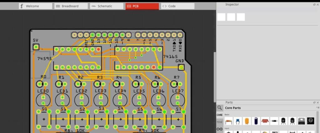
The first step in designing a PCB circuit online is creating a schematic. This involves drawing the circuit diagram using a software tool that is specifically designed for this purpose. Some popular software tools for creating schematics include Eagle, KiCAD, and Altium Designer.
When creating a schematic, it’s important to ensure that all the components are properly connected and that the circuit operates as intended. This involves checking the circuit for errors and making any necessary changes before moving on to the next step.
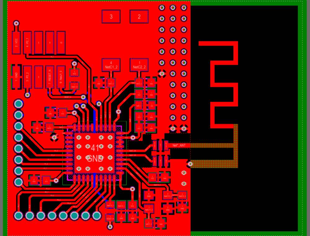
Layout Design
Once the schematic is complete, the next step is to design the layout of the PCB. This involves placing the components on the board and determining their placement and orientation. The layout design should take into account the size of the board, the number of components, and any other factors that may impact the final product.
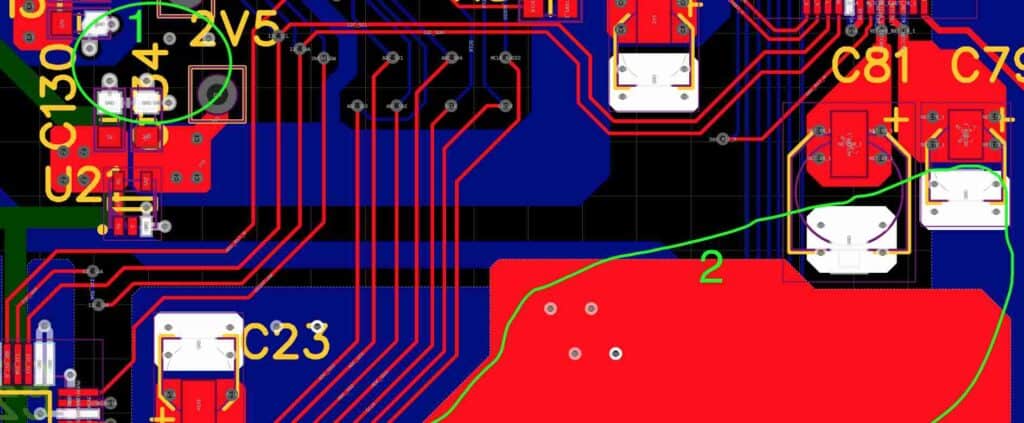
Routing
After the layout design is complete, the next step is routing. This involves connecting the components on the board using copper traces. The routing process can be automated using software tools, which can save time and improve accuracy.
When routing, it’s important to ensure that the traces are properly spaced and that there are no errors or overlaps. This can be done using a design rule check.
Design Rule Check
The final step in designing a PCB circuit online is the design rule check. This involves checking the design against a set of rules and constraints to ensure that it meets the required standards. The design rule check can be automated using software tools, which can help to identify any errors or issues that need to be addressed.
In conclusion, designing a PCB circuit online involves several steps, including creating a schematic, layout design, routing, and design rule check. Each of these steps is critical to the success of the final product, and it’s important to ensure that each step is completed accurately and thoroughly.
Collaborating and Sharing PCB Designs Online
Collaborating and sharing PCB designs online is an essential part of the PCB design process. It allows multiple users to work on the same design simultaneously, which can significantly reduce the time and effort required to complete a project. Here are some ways to collaborate and share PCB designs online:
1. Online Collaboration Tools
There are many online collaboration tools available that can help you collaborate with other team members on a PCB design project. These tools allow you to share design files, communicate with team members, and track changes in real-time. Some popular online collaboration tools for PCB design include Altium 365, CircuitMaker, and Upverter.
2. Version Control
Version control is essential when collaborating on PCB design projects. It allows you to keep track of changes made to the design and revert to previous versions if necessary. Git is a popular version control system that can be used for PCB design projects. It allows you to create branches, merge changes, and collaborate with other team members.
3. Online Design Communities
Online design communities such as GitHub and Hackaday can be an excellent resource for collaborating and sharing PCB designs online. These communities allow you to share your designs with others, get feedback, and collaborate with other designers. They can also be a great place to find inspiration for your next PCB design project.
4. Design Sharing Platforms
Design sharing platforms such as OSH Park and PCBWay allow you to share your PCB designs with others and have them manufactured. These platforms can be a great way to get feedback on your designs and connect with other designers who may be interested in collaborating on future projects.
In conclusion, collaborating and sharing PCB designs online can be a great way to save time and effort on your next PCB design project. By using online collaboration tools, version control systems, online design communities, and design sharing platforms, you can work with other team members to create high-quality PCB designs.
Common Mistakes to Avoid in PCB Circuit Design Online
Designing a printed circuit board (PCB) online can be an efficient and cost-effective way to create custom PCBs. However, there are some common mistakes that designers should avoid to ensure that their PCBs function properly and meet their design requirements.
1. Not Checking Design Rules
One of the most common mistakes in PCB circuit design is not checking the design rules. Design rules are the constraints that govern the layout of the PCB, such as minimum trace width, minimum clearance, and maximum via size. Failing to check the design rules can result in a PCB that does not function properly or that is not manufacturable.
2. Overcrowding the PCB
Another common mistake is overcrowding the PCB. It can be tempting to try to fit as many components as possible onto a PCB, but this can lead to problems such as signal interference, thermal issues, and difficulty in routing traces. It’s important to leave enough space between components to ensure proper functionality and manufacturability.
3. Ignoring Signal Integrity
Signal integrity is an important consideration in PCB circuit design. It refers to the ability of a signal to travel from one point on the PCB to another without distortion or loss of signal quality. Ignoring signal integrity can result in problems such as noise, crosstalk, and signal reflections.
4. Not Considering Manufacturing Constraints
Designers should also consider manufacturing constraints when designing a PCB. This includes factors such as the number of layers, the type of materials used, and the manufacturing process. Not considering these constraints can result in a PCB that is difficult or impossible to manufacture.
In conclusion, avoiding these common mistakes can help ensure that a PCB designed online functions properly and meets its design requirements. By checking design rules, avoiding overcrowding, considering signal integrity, and taking manufacturing constraints into account, designers can create high-quality PCBs that meet their needs.
