PCB design and fabrication are critical processes in the production of electronic devices. PCBs, or printed circuit boards, are the backbone of most electronic devices, providing a platform for the components to be mounted and connected. The design and fabrication of PCBs require a deep understanding of the principles of electronics, as well as the manufacturing processes involved.
The design process involves creating a schematic of the circuit, which is then translated into a physical layout of the PCB. This layout is then sent to the fabrication process, where the PCB is manufactured using a variety of techniques such as etching, drilling, and plating. The quality of the PCB design and fabrication can have a significant impact on the performance and reliability of the final product, making it a critical aspect of electronic device production.
In this article, we will explore the world of PCB design and fabrication, discussing the various techniques and processes involved. We will also delve into the importance of proper design and fabrication techniques, and how they can impact the performance and reliability of electronic devices. Whether you are a seasoned electronics professional or a hobbyist, understanding the principles of PCB design and fabrication is essential for success in the world of electronics.
PCB Design
PCB design is a crucial aspect of electronics manufacturing. It involves creating a blueprint of the circuit board that will be used to fabricate the final product. The design process is divided into three main stages: schematic capture, layout design, and design rule check (DRC).
Schematic Capture
Schematic capture is the first stage of PCB design. It involves creating a graphical representation of the circuit using a software tool. The schematic captures the electrical connections between the components, the values of the components, and any other relevant information.
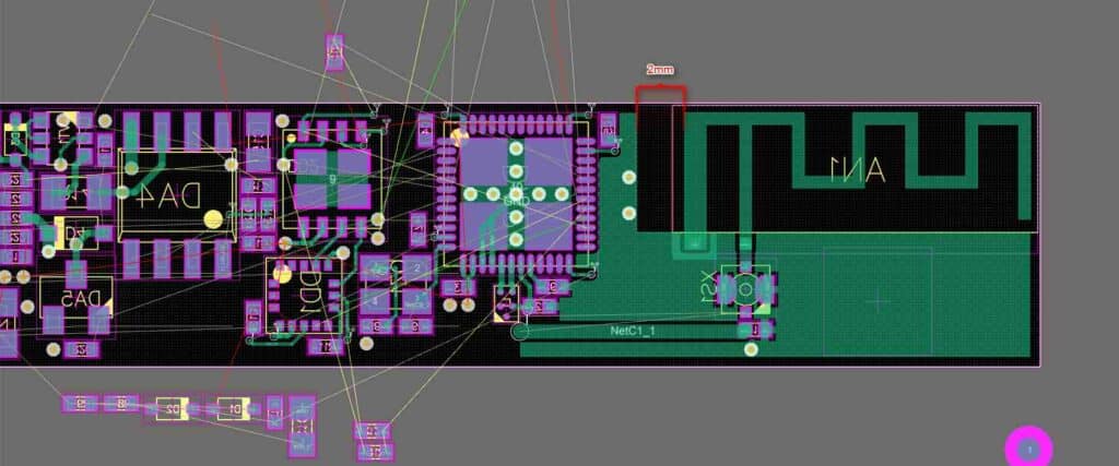
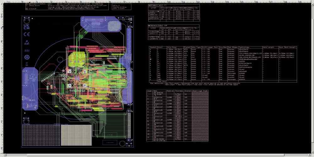
Layout Design
Layout design is the second stage of PCB design. It involves arranging the components on the circuit board and creating the physical layout of the board. The layout design takes into account the size and shape of the board, the placement of the components, and the routing of the traces that connect the components.
Design Rule Check (DRC)
Design rule check (DRC) is the final stage of PCB design. It involves validating the design against a set of rules and constraints. The DRC ensures that the design meets the requirements for manufacturing, such as minimum trace width and clearance, minimum drill size, and minimum annular ring size.
In conclusion, PCB design is an essential part of electronics manufacturing. The process involves schematic capture, layout design, and design rule check (DRC). Each stage is critical to ensuring that the final product meets the required specifications.
PCB Fabrication
When it comes to designing and manufacturing electronic devices, Printed Circuit Boards (PCBs) are an essential component. PCBs are used to connect electronic components, provide power, and facilitate communication between different parts of the device. In this section, we will discuss the PCB fabrication process, PCB material selection, and PCB assembly.
Printed Circuit Board (PCB) Manufacturing Process
The PCB manufacturing process involves several steps, including designing the PCB layout, printing the design onto the copper-clad board, etching the board to remove the unwanted copper, drilling holes for components, and finally, plating the board with a layer of metal to protect it from corrosion.
The first step in the PCB manufacturing process is designing the PCB layout using specialized software. Once the design is complete, it is printed onto the copper-clad board using a process called photolithography. The board is then etched to remove the unwanted copper, leaving only the traces that will connect the components.
After etching, the board is drilled to create holes for the components. The holes are then plated with a layer of metal to protect them from corrosion and provide a solid connection for the components.
PCB Material Selection
Choosing the right PCB material is crucial for the performance and reliability of the device. The most common materials used for PCBs are FR-4 (a type of fiberglass), polyimide, and Rogers materials. Each material has its own unique properties, such as thermal conductivity, dielectric constant, and mechanical strength.
FR-4 is the most widely used PCB material due to its low cost and high performance. Polyimide is more expensive but has excellent thermal stability and flexibility, making it ideal for applications where the board will be subjected to high temperatures or bending. Rogers materials are used for high-frequency applications due to their low dielectric constant and loss.
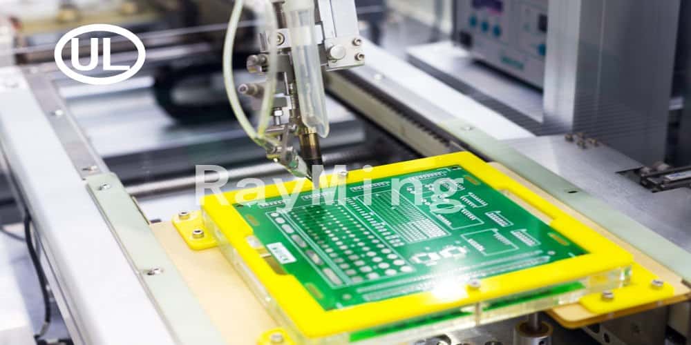
PCB Assembly
Once the PCB is fabricated, the components must be assembled onto the board. This process involves placing the components onto the board and soldering them in place. There are two main methods of PCB assembly: through-hole and surface mount.
Through-hole assembly involves inserting the component leads into pre-drilled holes on the board and soldering them in place. Surface mount assembly, on the other hand, involves soldering the components onto the surface of the board. Surface mount assembly is faster and more efficient but requires specialized equipment and expertise.
In conclusion, PCB fabrication is a complex process that involves several steps, including designing the layout, printing the design onto the board, etching, drilling, and plating the board. Choosing the right PCB material is crucial for the performance and reliability of the device, and the PCB assembly process involves placing and soldering components onto the board.
PCB Testing
When it comes to PCB design and fabrication, testing is a critical step to ensure the quality and functionality of the board. There are two main types of testing: electrical testing and functional testing.
PCB Electrical Testing
Electrical testing is performed to verify that the PCB meets the electrical specifications and requirements. This type of testing checks for any shorts, opens, or other electrical issues that may cause the board to malfunction. The following are the most common electrical tests:
- Continuity test: checks for any breaks in the circuit.
- Resistance test: measures the resistance of the traces and components.
- Capacitance test: measures the capacitance of the capacitors.
- Insulation resistance test: measures the insulation resistance between the traces and the ground.
PCB Functional Testing
Functional testing is performed to verify that the PCB performs its intended functions correctly. This type of testing checks for any software or hardware issues that may cause the board to malfunction. The following are the most common functional tests:
- Power-up test: checks if the board powers up correctly.
- Signal integrity test: checks if the signals are transmitted and received correctly.
- Software test: checks if the software runs correctly and produces the expected output.
- Environmental test: checks if the board can withstand the environmental conditions it will be exposed to.
In conclusion, PCB testing is a crucial step in ensuring the quality and functionality of the board. By performing both electrical and functional testing, designers and manufacturers can catch any issues before the board is released to the market.
PCB Design Tools
PCB Design Software
PCB design software is an essential tool for designing and laying out printed circuit boards. It is used to create the schematic diagram, route the traces, and generate the Gerber files that are used in the fabrication process. There are many different PCB design software packages available, each with its own set of features and capabilities.
Some popular PCB design software packages include:
- Altium Designer
- Eagle PCB Design
- KiCAD
- OrCAD
- PADS PCB Design
- CircuitMaker
Each software package has its own strengths and weaknesses, and the choice of software will depend on the specific needs of the designer. Some software packages are better suited for complex designs, while others are more user-friendly and easier to learn.
PCB Design Standards
PCB design standards are a set of guidelines that ensure that printed circuit boards are designed and fabricated to meet specific requirements. These standards cover everything from the size and shape of the board to the placement of components and the routing of traces.
Some common PCB design standards include:
- IPC-2221A – Generic Standard on Printed Board Design
- IPC-2222 – Sectional Design Standard for Rigid Organic Printed Boards
- IPC-2223 – Sectional Design Standard for Flexible Printed Boards
- IPC-6012 – Qualification and Performance Specification for Rigid Printed Boards
Following these standards is important for ensuring that the finished PCB meets the requirements for its intended use. It also helps to ensure that the PCB can be manufactured efficiently and reliably.
In conclusion, PCB design tools are an essential part of the PCB design and fabrication process. PCB design software allows designers to create schematics, route traces, and generate Gerber files, while PCB design standards ensure that the finished product meets specific requirements. By using these tools and following established standards, designers can create high-quality PCBs that meet the needs of their customers.
PCB Design Best Practices
PCB Layout Guidelines
When designing a PCB layout, there are a few best practices to keep in mind to ensure a successful design. First, it’s important to consider the physical layout of the board, including the placement of components, traces, and vias. Components should be placed in a logical, organized manner, with consideration for signal flow and ease of assembly. Traces should be kept as short as possible to minimize signal loss and interference, and vias should be placed strategically to avoid signal crosstalk.
Another important consideration is the use of ground planes. Ground planes help to reduce noise and interference, and can also help to dissipate heat. When designing a PCB, it’s a good idea to include a ground plane on at least one layer of the board.
PCB Design for Manufacturability (DFM)
Designing a PCB for manufacturability is essential to ensuring that the board can be produced efficiently and cost-effectively. When designing a PCB, it’s important to take into account the capabilities of the manufacturer, including their preferred board thickness, minimum trace width and spacing, and drill sizes.
It’s also important to consider the placement of components and the use of surface mount technology (SMT) versus through-hole components. SMT components are generally preferred for their smaller size and ease of assembly, but through-hole components may be necessary for certain applications.
Finally, it’s important to consider the use of copper pours and the placement of fiducials. Copper pours can help to reduce noise and interference, while fiducials can help to ensure accurate placement of components during assembly.
In conclusion, following these PCB design best practices can help to ensure a successful and manufacturable design.
Conclusion
In conclusion, PCB design and fabrication is a crucial aspect of electronic device development. It involves the creation of a design that meets the specifications of the device and the selection of the right materials and components to ensure optimal performance.
The process of PCB fabrication has evolved over the years, with the introduction of new technologies and techniques that have made it easier and more efficient. The use of computer-aided design (CAD) software, for instance, has made it possible to create accurate and precise designs in a shorter time frame.
When it comes to selecting a PCB fabrication service, it is important to consider factors such as quality, cost, and lead time. It is also important to choose a service provider that has a proven track record of delivering high-quality PCBs that meet your specific requirements.
Overall, PCB design and fabrication is a complex process that requires careful planning and attention to detail. By working with the right PCB fabrication service, you can ensure that your electronic device is built to the highest standards of quality and performance.
