Table of Contents
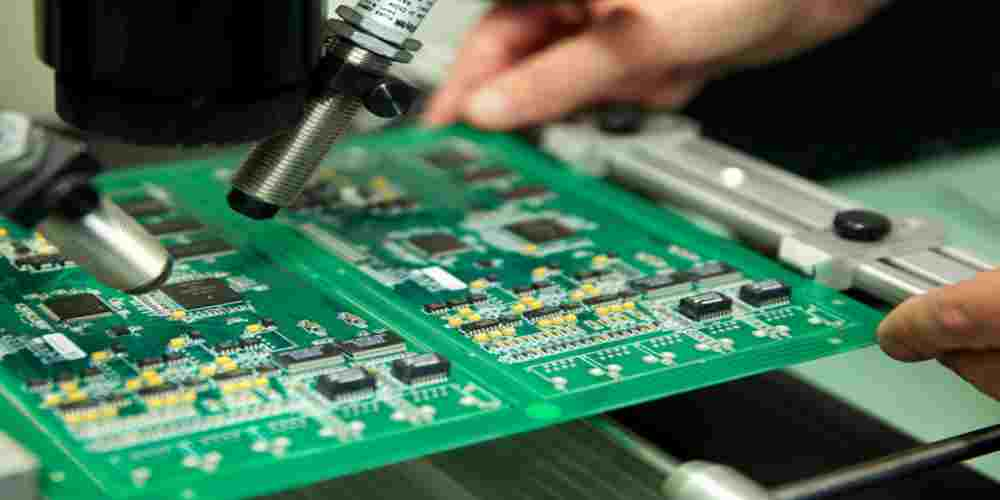
TogglePCB layout printing is an essential part of the printed circuit board manufacturing process. It involves designing and arranging the components and circuitry onto the board, ensuring that the electrical connections are proper and efficient. The layout of the PCB is crucial, as it determines the performance and reliability of the final product.
In the past, PCB layout printing was a time-consuming and laborious process. However, with the advancement of technology, it has become easier and more efficient. Nowadays, software programs are available that can help designers create the layout quickly and accurately. These programs offer a range of features such as auto-routing, design rule checks, and 3D visualization, which make the process more streamlined and error-free.

Basics of PCB Layout Printing
PCB Layout Printing Process
PCB layout printing is a crucial step in the process of creating printed circuit boards. The process involves transferring the design of the circuit onto a copper-clad board. The board is then etched to remove the unwanted copper, leaving behind the printed circuit.
The process of PCB layout printing involves the following steps:
- Design the circuit using a PCB design software.
- Print the design onto transfer paper using a laser printer.
- Transfer the design onto the copper-clad board using a heat press.
- Etch the board to remove unwanted copper.
- Clean the board to remove any remaining transfer paper.
Tools and Materials Required
To perform PCB layout printing, you will need the following tools and materials:
- PCB design software
- Laser printer
- Transfer paper
- Copper-clad board
- Heat press
- Etchant solution
- Protective gloves and goggles
- Cleaning solution
- Brushes
Design Considerations
When designing a PCB for layout printing, there are several considerations to keep in mind. These include:
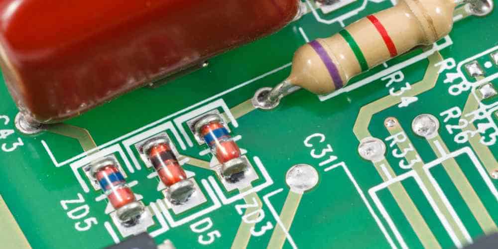
- Component placement: Ensure that the components are placed in a logical and efficient manner to minimize the length of traces and reduce the risk of interference.
- Trace width and spacing: The width and spacing of the traces should be appropriate for the current and voltage levels of the circuit.
- Ground plane: A ground plane can help reduce noise and interference in the circuit.
- Signal integrity: Ensure that the traces are routed in a way that maintains the signal integrity of the circuit.
In conclusion, PCB layout printing is an essential step in the process of creating printed circuit boards. By following the right process and using the appropriate tools and materials, you can create high-quality PCBs that meet your design requirements.
PCB Layout Printing Techniques

When it comes to printing PCB layouts, there are a few different techniques that you can use depending on your needs and resources. In this section, we will explore three common methods: screen printing, inkjet printing, and laser printing.
Screen Printing
Screen printing is a traditional method of printing that involves using a mesh screen to transfer ink onto a surface. To use this technique for PCB layout printing, you will need to create a stencil of your layout and then use it to apply ink to the board. This method is best suited for larger designs and can produce high-quality results with consistent ink coverage.
Inkjet Printing
Inkjet printing is a popular method of printing that involves using a printer to apply ink directly onto the surface of the board. This method is best suited for smaller designs and can produce high-resolution prints with precise detail. However, inkjet printers can be expensive and the ink can be prone to smudging or fading over time.
Laser Printing
Laser printing is another popular method of printing that involves using a laser printer to transfer toner onto the surface of the board. This method is best suited for medium-sized designs and can produce high-quality prints with sharp lines and clear text. However, laser printers can also be expensive and may require additional equipment such as a laminator to transfer the toner onto the board.
Overall, the choice of PCB layout printing technique will depend on your specific needs and resources. Each method has its own advantages and disadvantages, and it is important to choose the one that best suits your project requirements.
Advanced PCB Layout Printing
Multilayer PCB Printing
Multilayer PCBs consist of multiple layers of conductive material separated by insulating layers. To print multilayer PCBs, manufacturers use a process called lamination. During lamination, they bond the layers together using heat and pressure. The process requires precise alignment to ensure the layers match up correctly. Manufacturers often use optical alignment systems to achieve this.
SMT Stencil Printing
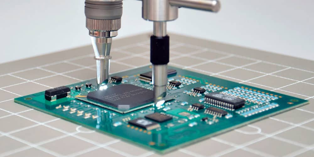
Surface Mount Technology (SMT) stencils are used to apply solder paste to the surface of a PCB. The solder paste holds the SMT components in place during the soldering process. To print SMT stencils, manufacturers use a process called laser cutting. The process involves using a laser to cut a pattern into a metal sheet. The pattern corresponds to the layout of the PCB. The stencil is then aligned with the PCB and the solder paste is applied.
Flex PCB Printing
Flex PCBs are designed to bend and flex without breaking. They are made using a flexible material like polyimide. To print flex PCBs, manufacturers use a process called screen printing. The process involves using a stencil to apply a conductive ink to the flexible material. The ink is then cured using heat to create the conductive traces.
In conclusion, advanced PCB layout printing involves printing multilayer PCBs, SMT stencils, and flex PCBs. These processes require precise alignment and use techniques like lamination, laser cutting, and screen printing. By understanding these processes, manufacturers can produce high-quality PCBs that meet the needs of their customers.
Common Mistakes in PCB Layout Printing

Design Errors
Design errors are common mistakes that can be made in the initial stages of PCB layout printing. These errors can lead to significant problems in the final product. Some common design errors include:
- Incorrect component placement
- Poor trace routing
- Improper ground plane design
- Inadequate spacing between components
- Inconsistent trace widths
To avoid design errors, it is important to thoroughly review the design before moving on to the printing stage. Double-check all component placements and trace routing to ensure that everything is properly spaced and aligned.
Printing Errors
Printing errors can occur during the actual printing process. These errors can be caused by a variety of factors, including:
- Poor ink quality
- Improper printing settings
- Inadequate printer calibration
- Incorrect printing temperature
To avoid printing errors, it is important to use high-quality ink and ensure that the printer is properly calibrated. Double-check all printing settings before beginning the printing process.
Post-Printing Errors
Post-printing errors can occur during the final stages of PCB layout printing. These errors can be caused by a variety of factors, including:
- Inadequate curing time
- Improper handling of the PCB
- Poor quality control
To avoid post-printing errors, it is important to follow proper curing times and handle the PCB with care. Additionally, it is important to implement quality control measures to ensure that the final product meets all necessary standards.
Overall, avoiding common mistakes in PCB layout printing requires careful attention to detail and a thorough understanding of the printing process. By taking the time to review designs, use high-quality materials, and follow proper procedures, it is possible to create high-quality PCBs that meet all necessary standards.
Conclusion

In conclusion, PCB layout printing is a critical process that requires attention to detail and precision. It involves creating a design that is both functional and aesthetically pleasing. Throughout this article, we have discussed the various aspects of PCB layout printing, including the design process, software tools, and techniques.
One of the most important factors to consider when designing a PCB layout is the placement of components. It is essential to ensure that all components are placed in the correct location and orientation to ensure proper functionality. Additionally, the spacing between components must be carefully considered to avoid interference and signal loss.
Another critical aspect of PCB layout printing is the use of software tools. There are many software tools available that can help streamline the design process and improve efficiency. Some of the most popular software tools include Altium Designer, Eagle PCB, and KiCad.
Finally, it is essential to use the proper printing techniques to ensure that the final product is of high quality. This includes using the correct printing materials, such as copper foil and solder mask, and ensuring that the printing process is done accurately and precisely.
Overall, PCB layout printing is a complex process that requires knowledge, skill, and attention to detail. By following the tips and techniques outlined in this article, you can create high-quality PCB layouts that meet your design requirements and specifications.

