Prototype PCB fabrication is the process of creating a small-scale printed circuit board (PCB) to test and validate a design before mass production. It is an essential step in the development of electronic devices, as it allows engineers to identify and correct any issues with the design before investing in expensive mass production.
The process of prototype PCB fabrication involves several steps, including designing the circuit schematic, laying out the PCB design, and manufacturing the board. The design process begins with the creation of a schematic diagram that outlines the components and connections of the circuit. This is followed by the layout of the PCB design, which involves placing the components and routing the traces to create a functional circuit. Finally, the board is manufactured using various techniques, such as etching, milling, or printing.
Prototype PCB fabrication is a critical step in the development of electronic devices, as it allows engineers to test and refine their designs before committing to mass production. By identifying and correcting issues early in the design process, engineers can save time and money while ensuring that their final product meets the required specifications. With the increasing demand for smaller, more complex electronic devices, the importance of prototype PCB fabrication is only set to grow in the coming years.
Benefits of Prototype PCB Fabrication
Prototype PCB fabrication offers numerous benefits for engineers and designers who are working on new and innovative projects. Here are some of the key advantages of using prototype PCB fabrication:
Faster Time to Market
One of the biggest benefits of prototype PCB fabrication is that it allows engineers and designers to quickly iterate on their designs and get their products to market faster. With rapid prototyping techniques, it’s possible to create fully functional prototypes in a matter of days, rather than weeks or months.
Cost Savings
Another advantage of prototype PCB fabrication is that it can help save money in the long run. By catching design flaws early in the process, engineers can avoid costly mistakes and rework down the line. Additionally, by producing small batches of prototypes, designers can test their products in the real world before committing to a full production run.
Customization
Prototype PCB fabrication also allows for a high degree of customization. With the ability to produce small batches of prototypes, engineers and designers can experiment with different designs and features to find the best solution for their product. This flexibility can lead to better products and happier customers.
Improved Quality
Finally, prototype PCB fabrication can lead to improved product quality. By catching design flaws early in the process, engineers can ensure that their final product meets all of their requirements and specifications. Additionally, by testing their prototypes in the real world, designers can identify and address any issues before they become major problems.
In conclusion, prototype PCB fabrication offers numerous benefits for engineers and designers who are working on new and innovative projects. By providing faster time to market, cost savings, customization, and improved quality, it’s a valuable tool for anyone looking to bring their ideas to life.
Common Materials Used for Prototype PCB Fabrication

Rigid PCB Materials
Rigid PCBs are the most common type of PCBs and are widely used in electronic devices. The most common materials used for rigid PCB fabrication are:
- FR-4: This is a fiberglass-reinforced epoxy laminate that is widely used in PCB manufacturing due to its high strength and excellent electrical properties. It is also cost-effective and readily available.
- Aluminum: Aluminum PCBs are used in applications where heat dissipation is critical, such as LED lighting and power supplies. They have a high thermal conductivity and are lightweight.
- Ceramic: Ceramic PCBs are used in high-frequency applications due to their excellent electrical properties. They are also highly durable and can withstand high temperatures.
Flexible PCB Materials
Flexible PCBs, also known as flex PCBs, are used in applications where space is limited or where the PCB needs to conform to a specific shape. The most common materials used for flexible PCB fabrication are:
- Polyimide: Polyimide is a popular material for flexible PCBs due to its high temperature resistance and flexibility. It is also lightweight and has excellent electrical properties.
- Polyester: Polyester is a cost-effective alternative to polyimide and is widely used in consumer electronics. It has good electrical properties and is easy to process.
- Liquid Crystal Polymer (LCP): LCP is a high-performance material that is used in applications where high-frequency signals are required. It has excellent electrical properties and is highly durable.
In conclusion, the choice of PCB material depends on the specific requirements of the application. PCB designers should carefully consider the electrical, mechanical, and thermal properties of the material before making a decision.
Prototype PCB Fabrication Process
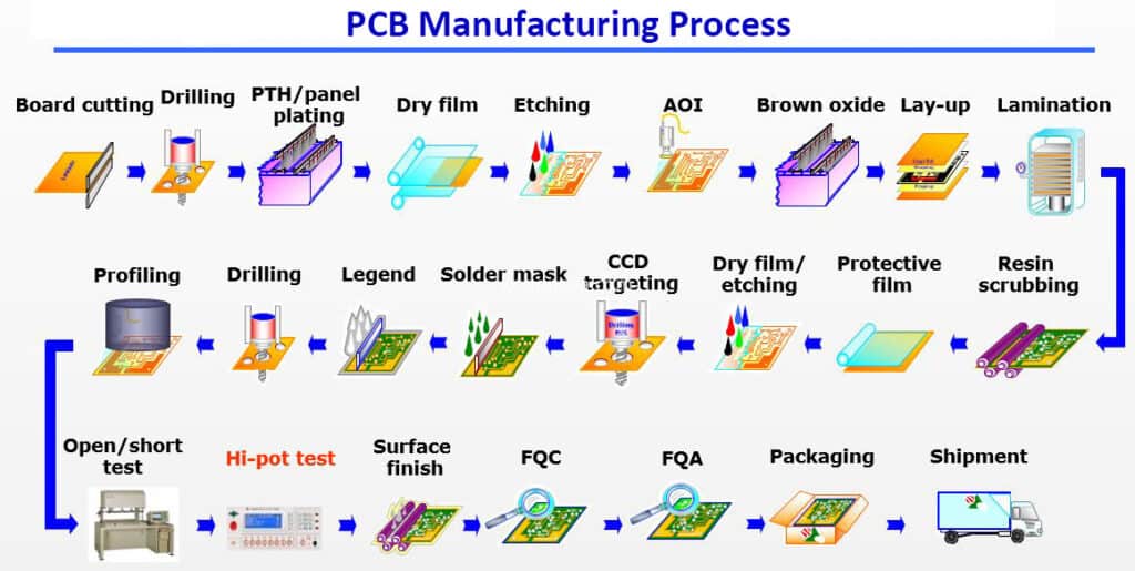
Designing the PCB Layout
The first step in prototype PCB fabrication is designing the PCB layout. This involves using a computer-aided design (CAD) software to create a digital representation of the printed circuit board. The layout must be designed with the correct dimensions and specifications to ensure that the PCB functions as intended.
Printing the PCB Layout
Once the PCB layout is designed, it must be printed onto a special type of paper or film. This is done using a laser printer or inkjet printer that is capable of producing high-quality prints. The printed layout is then transferred onto the copper-clad board.
Etching the PCB
Etching is the process of removing unwanted copper from the board to create the circuit pattern. This is done by applying a chemical solution to the board that dissolves the copper in the areas where it is not needed. The remaining copper forms the conductive traces that make up the circuit.
Drilling and Plating the PCB
After the etching process, the board is drilled to create holes for the components. These holes are then plated with a thin layer of copper to ensure a good electrical connection between the component leads and the conductive traces on the board.
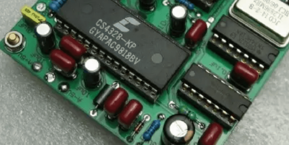
Soldering Components to the PCB
The final step in prototype PCB fabrication is soldering the components to the board. This involves using a soldering iron to heat the component leads and melt the solder, which then flows onto the conductive traces and forms a strong electrical connection.
In summary, prototype PCB fabrication involves designing the PCB layout, printing the layout onto the board, etching the board to create the circuit pattern, drilling and plating the board to create holes for the components, and finally soldering the components to the board.
Quality Control in Prototype PCB Fabrication
Quality control is a crucial aspect of prototype PCB fabrication. It ensures that the final product meets the required specifications and performs as expected. There are several quality control measures that are implemented during the fabrication process.
One of the primary quality control measures is the inspection of the raw materials. The quality of the materials used in the fabrication process has a significant impact on the final product’s performance. Therefore, it is essential to inspect the materials before they are used in the fabrication process.
Another important quality control measure is the inspection of the PCB layout design. Before the PCB is fabricated, the layout design is inspected to ensure that it meets the required specifications. The layout design is checked for errors such as incorrect component placement, incorrect trace widths, and incorrect spacing between components.
During the fabrication process, the PCB is inspected at various stages to ensure that it is being fabricated according to the design specifications. The inspection includes checking the thickness of the copper layers, the size of the holes, and the placement of the components.
After the PCB is fabricated, it undergoes a final inspection to ensure that it meets the required specifications. The inspection includes checking the PCB’s dimensions, the thickness of the copper layers, and the placement of the components.
In conclusion, quality control is a crucial aspect of prototype PCB fabrication. It ensures that the final product meets the required specifications and performs as expected. The quality control measures implemented during the fabrication process include the inspection of raw materials, inspection of the PCB layout design, inspection during the fabrication process, and final inspection.
Choosing a Prototype PCB Fabrication Service
When it comes to choosing a prototype PCB fabrication service, there are various factors to consider. The right service can help you create high-quality, reliable circuit boards that meet your specific needs. Here are some factors to consider when choosing a prototype PCB fabrication service:
Factors to Consider
-
Experience: Look for a service with a proven track record of delivering high-quality circuit boards. Check their portfolio, customer reviews, and testimonials to ensure they have experience in your industry and can meet your specific requirements.
-
Capabilities: Consider the range of capabilities offered by the service, such as the types of materials used, the number of layers supported, and the ability to produce boards with fine pitch components. Make sure the service can meet your specific needs and requirements.
-
Turnaround time: Time is of the essence when it comes to PCB fabrication. Look for a service that can deliver your circuit boards within your desired timeframe without compromising on quality.
-
Cost: PCB fabrication can be expensive, especially for complex designs. Look for a service that offers competitive pricing without compromising on quality.
Popular Prototype PCB Fabrication Services
Here are some popular prototype PCB fabrication services to consider:
-
JLCPCB: A China-based service that offers a range of capabilities, including up to 16 layers, 3 mil trace and space, and a range of materials. They offer competitive pricing and fast turnaround times.
-
PCBWay: Another China-based service that offers a range of capabilities, including up to 14 layers, 4 mil trace and space, and a range of materials. They offer competitive pricing and a range of delivery options.
-
Oshpark: A US-based service that specializes in small-batch PCB fabrication. They offer a range of capabilities, including up to 4 layers, 6 mil trace and space, and a range of materials. They offer competitive pricing and fast turnaround times.
Choosing the right prototype PCB fabrication service can make all the difference in the success of your project. Consider these factors and popular services to find the right fit for your needs.
