Schematic design PCB, also known as printed circuit board design, is a crucial step in the development of electronic devices. It involves the creation of a visual representation of the circuitry that will be used in the device. This design is then used to manufacture the actual PCB, which serves as the foundation for the electronic device.
The schematic design PCB process involves the use of specialized software to create a digital representation of the circuitry. This design is then reviewed and refined to ensure that it meets the requirements of the device. Once the design is finalized, it is used to create the physical PCB, which is then populated with the necessary components to create the electronic device. The schematic design PCB process is a critical step in the development of electronic devices, as it ensures that the circuitry is designed to meet the specific needs of the device and that it can be manufactured efficiently and cost-effectively.
Basics of Schematic Design PCB
What is a Schematic Design PCB?
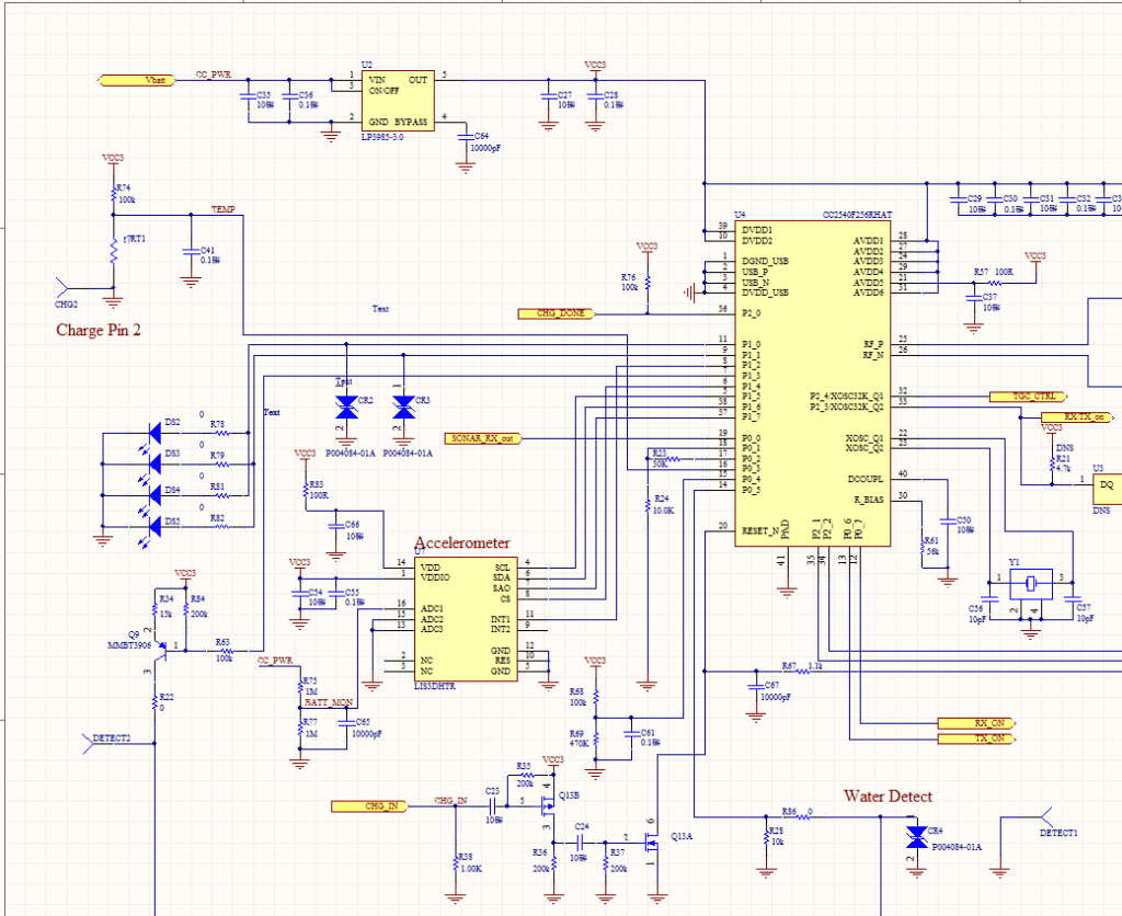
A schematic design PCB is a graphical representation of an electronic circuit. It shows the components used in the circuit and the connections between them. It is a fundamental step in the electronic design process and is used to communicate the design to others, such as engineers, technicians, and manufacturers.
Why is Schematic Design PCB important?
Schematic design PCB is important for several reasons. Firstly, it allows designers to visualize the circuit and identify potential problems before the circuit is built. This can save time and money by avoiding mistakes that could be costly to fix. Secondly, it enables designers to communicate the design to others, such as engineers, technicians, and manufacturers. This is important because it ensures that everyone involved in the design process understands the design and can work together to build it. Finally, it provides a record of the design that can be used for future reference or modification.
In summary, schematic design PCB is a crucial step in the electronic design process. It enables designers to visualize and communicate the design, identify potential problems, and provide a record of the design for future reference.
Components Used in Schematic Design PCB
When designing a printed circuit board (PCB), the schematic design is crucial. The schematic design is a graphical representation of the circuit that shows how the components are connected. It is the blueprint for the PCB layout. In this section, we will discuss the components used in schematic design PCB.
Resistors
Resistors are passive components that resist the flow of current. They are used to control the amount of current flowing through a circuit. Resistors come in different values and sizes. The value of a resistor is measured in ohms (Ω). The size of a resistor is indicated by its physical size and power rating.
Capacitors
Capacitors are passive components that store electrical charge. They are used to filter out unwanted signals or to store energy. Capacitors come in different types, such as ceramic, electrolytic, and tantalum. The value of a capacitor is measured in farads (F). The size of a capacitor is indicated by its physical size and voltage rating.
Inductors
Inductors are passive components that store energy in a magnetic field. They are used to filter out unwanted signals or to store energy. Inductors come in different types, such as air-core, iron-core, and ferrite-core. The value of an inductor is measured in henries (H). The size of an inductor is indicated by its physical size and current rating.
Transistors
Transistors are active components that amplify or switch electronic signals. They come in different types, such as bipolar junction transistor (BJT) and field-effect transistor (FET). The transistor has three terminals: the emitter, the base, and the collector. The transistor is used in many applications, such as amplifiers, oscillators, and digital circuits.
Diodes
Diodes are passive components that allow current to flow in one direction only. They are used to convert AC to DC or to protect circuits from reverse voltage. Diodes come in different types, such as rectifier diodes, zener diodes, and light-emitting diodes (LEDs). The value of a diode is measured in volts (V). The size of a diode is indicated by its physical size and power rating.
Integrated Circuits
Integrated circuits (ICs) are complex electronic circuits that are miniaturized on a single chip. They contain many components, such as transistors, diodes, and resistors. ICs come in different types, such as digital ICs and analog ICs. They are used in many applications, such as microprocessors, memory chips, and communication circuits.
In conclusion, the components used in schematic design PCB are essential for the proper functioning of the circuit. Each component has its unique properties and functions. By understanding the properties and functions of each component, you can design a reliable and efficient circuit.
Tools and Software for Schematic Design PCB

When it comes to designing a printed circuit board (PCB), having the right tools and software can make all the difference. There are several options available for schematic design PCB, and each one has its own strengths and weaknesses. In this section, we will discuss the three main categories of software that are used in the PCB design process: schematic capture software, PCB layout software, and simulation software.
Schematic Capture Software
Schematic capture software is used to create the initial circuit diagram for the PCB. This software allows designers to create a visual representation of the circuit, including all of the components and their connections. Some of the most popular schematic capture software options include:
- Altium Designer
- Eagle PCB Design
- KiCAD
- OrCAD
- PSpice
Each of these options has its own unique features and pricing structures, so it is important to do your research and choose the one that best fits your needs.
PCB Layout Software
Once the schematic has been created, the next step is to lay out the actual PCB. PCB layout software is used to arrange the components on the board and create the physical design of the circuit. Some of the most popular PCB layout software options include:
Again, each of these options has its own unique features and pricing structures, so it is important to choose the one that best fits your needs.
Simulation Software
Simulation software is used to test the design of the circuit before it is actually built. This allows designers to identify any potential issues or problems before they become a reality. Some of the most popular simulation software options include:
- SPICE
- LTSpice
- Multisim
- PSpice
Simulation software can be incredibly helpful in the PCB design process, but it is important to keep in mind that simulations are not always 100% accurate. It is still important to physically test the circuit before it is put into use.
Overall, having the right tools and software is essential for successful schematic design PCB. By choosing the right options for your needs and being diligent in the design process, you can create a high-quality PCB that meets all of your requirements.
Designing a Schematic Design PCB
Creating a Schematic Diagram
The first step in designing a schematic design PCB is creating a schematic diagram. This diagram represents the circuit you want to build and includes all the components and connections between them. You can use software like Altium Designer, Eagle PCB, or KiCAD to create your schematic diagram.
When creating your schematic diagram, it is important to follow a few best practices. First, use clear and concise labels for all components and connections. Second, organize your diagram in a logical and easy-to-follow manner. Finally, use a consistent style throughout your diagram to make it easier to read and understand.
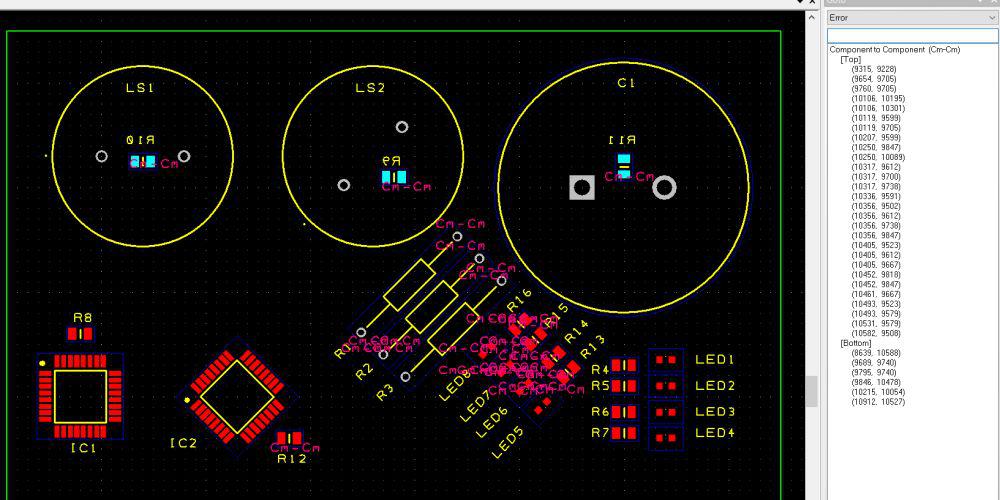
PCB Layout Design
Once you have created your schematic diagram, the next step is to design the PCB layout. This involves placing all the components from your schematic diagram onto a physical board and routing the connections between them.
When designing your PCB layout, you need to consider a few key factors. First, you need to ensure that all components fit onto the board and that there is enough space between them. Second, you need to consider the placement of components to minimize noise and interference. Finally, you need to route your connections in a way that minimizes signal loss and interference.
Design Rules Checking
Before you can generate Gerber files for your PCB, you need to perform design rule checking (DRC). This involves checking your design against a set of rules to ensure that it is manufacturable and meets all necessary specifications.
When performing DRC, you need to check for a few key factors. First, you need to ensure that all components are properly placed and routed. Second, you need to check for any design rule violations, such as overlapping traces or vias that are too close together. Finally, you need to check that your design meets all necessary specifications, such as minimum trace width and clearance.
Generating Gerber Files
Once you have completed your design and performed DRC, the final step is to generate Gerber files. These files contain all the necessary information for manufacturing your PCB, including the location of components, routing information, and drill holes.
When generating Gerber files, you need to ensure that you include all necessary layers, such as top and bottom copper, silkscreen, and solder mask. You also need to specify the correct board size and drill hole sizes. Finally, you need to ensure that your Gerber files are compatible with the manufacturing process you plan to use.
Overall, designing a schematic design PCB requires careful planning and attention to detail. By following best practices and performing thorough design rule checking, you can create a high-quality PCB that meets all necessary specifications.
Testing and Validation of Schematic Design PCB

Electrical Testing
Electrical testing of a PCB involves verifying the electrical connections and characteristics of the different components on the board. This is done to ensure that all components are functioning as intended and that there are no defects or errors in the design. Electrical testing is typically carried out using specialized equipment such as a multimeter or an oscilloscope.
During electrical testing, it is important to check the voltage and current levels at various points on the board. This helps to identify any potential issues such as short circuits, open circuits, or incorrect component values. Additionally, electrical testing can be used to verify the power supply and ground connections on the board.
Functional Testing
Functional testing involves verifying the overall functionality of the PCB. This is done by connecting the board to a power source and testing its performance under various operating conditions. Functional testing can be done using specialized equipment or by running specific test programs on the board.
During functional testing, it is important to verify that the board is performing as intended and that all components are functioning correctly. This includes checking the performance of any microcontrollers or other programmable components on the board.
Environmental Testing
Environmental testing involves subjecting the PCB to various environmental conditions to test its performance under different conditions. This can include testing the board’s performance under high or low temperatures, high humidity, or exposure to various chemicals or other substances.
Environmental testing is important to ensure that the board can withstand the conditions it may be exposed to during its intended use. This can help to identify any potential issues with the board’s design or components and ensure that it is suitable for its intended application.
Overall, testing and validation of a schematic design PCB is an important step in ensuring that the board is functioning correctly and is suitable for its intended application. By carrying out thorough testing and validation, designers can identify and correct any potential issues before the board is put into use.
Conclusion

In conclusion, schematic design is an essential aspect of PCB design. It helps in the creation of a blueprint that guides the layout of the board. This process involves a lot of attention to detail and accuracy to ensure that the final product meets the required standards.
Through schematic design, designers can easily identify the connections between components and ensure that they are correctly placed. This helps to minimize the risk of errors and reduce the time spent on troubleshooting.
Furthermore, schematic design allows for the integration of different components and modules, which is essential in the development of complex systems. It also enables the designer to optimize the layout of the board, resulting in a more compact and efficient design.
Overall, schematic design is an integral part of PCB design, and its importance cannot be overstated. It is crucial to ensure that the design is accurate, efficient, and meets the required standards. By paying attention to detail and utilizing the necessary tools, designers can create high-quality PCBs that meet the needs of their clients.
