5G technology is the latest advancement in wireless communication, and it promises to revolutionize the way we connect to the internet. With faster speeds, lower latency, and greater capacity, 5G networks will enable a whole new range of applications and services, from autonomous vehicles to virtual reality. But to make all of this possible, we need to design and build 5G circuit boards that can handle the demands of this new technology.
At the heart of any 5G device is a circuit board that contains the necessary components to transmit and receive signals. These components include antennas, amplifiers, filters, and other electronic components that work together to create a network that can support the high speeds and low latency of 5G. Designing a circuit board for 5G requires a deep understanding of the technology and the ability to optimize the layout and placement of components to minimize interference and maximize performance.
The design of a 5G circuit board is a complex process that involves a team of engineers working together to create a board that meets the specific requirements of the device it will be used in. From choosing the right materials to optimizing the layout and placement of components, every detail must be carefully considered to ensure that the board can handle the demands of 5G technology. With the right design, a 5G circuit board can unlock the full potential of this revolutionary technology and enable a new era of connectivity and innovation.
5G Circuit Board Design Basics
What is 5G Circuit Board Design?
5G circuit board design refers to the process of designing printed circuit boards (PCBs) that are optimized for 5G wireless networks. These PCBs are used in a wide range of devices, including smartphones, tablets, laptops, and other IoT devices.
The design of a 5G circuit board is critical to the overall performance of a device, as it directly affects the speed, reliability, and efficiency of the wireless connection. A well-designed 5G circuit board can help to minimize interference, reduce power consumption, and improve signal strength, which can lead to faster data transfer speeds and a better user experience.
Why is 5G Circuit Board Design Important?
The importance of 5G circuit board design cannot be overstated, as it directly impacts the performance and functionality of 5G devices. With the increasing demand for faster and more reliable wireless networks, the design of 5G circuit boards has become more crucial than ever.
One of the main challenges of 5G circuit board design is the need to support multiple frequency bands and technologies, which can be complex and difficult to implement. Additionally, 5G circuit boards must be designed to handle high data rates and low latency, which can be challenging due to the high frequency of the signals.
In summary, 5G circuit board design is a critical component of the development of 5G devices, and requires careful consideration and planning to ensure optimal performance.
Key Considerations for 5G Circuit Board Design

When designing a circuit board for 5G, there are several key considerations that must be taken into account. These include high-frequency design considerations, thermal management, material selection, signal integrity, and power integrity.
High-Frequency Design Considerations
One of the most important considerations for 5G circuit board design is high-frequency design. The higher frequencies used in 5G networks require careful attention to detail when it comes to circuit board layout, component placement, and signal routing. Some key high-frequency design considerations include:
- Minimizing signal loss and noise
- Reducing electromagnetic interference (EMI)
- Ensuring proper impedance matching
- Using high-quality components and materials
Thermal Management
Another important consideration for 5G circuit board design is thermal management. The higher frequencies used in 5G networks can result in increased heat generation, which can affect the performance and reliability of circuit boards. Some key thermal management considerations include:
- Proper component placement to maximize airflow
- Use of heat sinks, thermal pads, and other cooling solutions
- Careful attention to board layout to minimize heat buildup
Material Selection
The choice of materials used in 5G circuit board design is also critical. The materials used must be able to handle the high frequencies and temperatures associated with 5G networks. Some key material selection considerations include:
- Choosing materials with low dielectric loss
- Selecting materials with high thermal conductivity
- Ensuring materials are compatible with high-frequency signals
Signal Integrity
Signal integrity is another important consideration for 5G circuit board design. High-frequency signals can be easily degraded by noise, interference, and other factors. Some key signal integrity considerations include:
- Minimizing signal loss and noise
- Ensuring proper impedance matching
- Using high-quality components and materials
Power Integrity
Finally, power integrity is another important consideration for 5G circuit board design. The high frequencies used in 5G networks can result in power fluctuations that can affect circuit board performance and reliability. Some key power integrity considerations include:
- Proper power supply design and layout
- Use of decoupling capacitors and other filtering solutions
- Careful attention to board layout to minimize power fluctuations
Overall, designing a circuit board for 5G requires careful attention to detail and a thorough understanding of the unique challenges posed by high-frequency networks. By taking into account these key considerations, designers can create circuit boards that are reliable, efficient, and capable of meeting the demands of 5G networks.
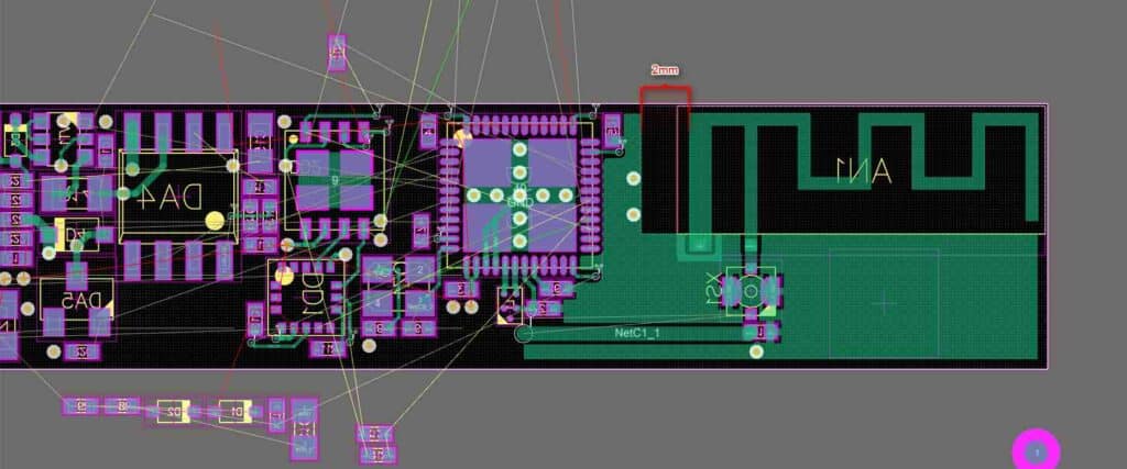
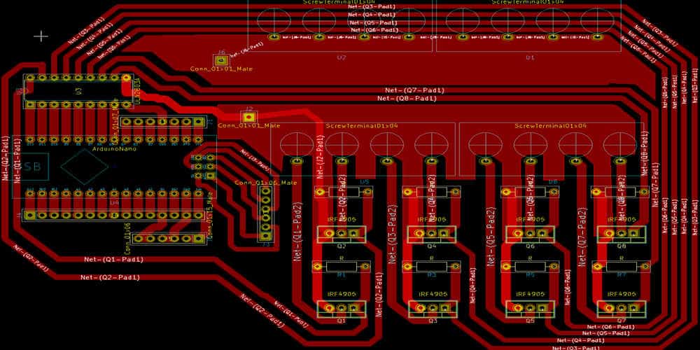
Design Tools and Software for 5G Circuit Board Design
EDA Tools
EDA (Electronic Design Automation) tools are essential for designing and analyzing 5G circuit boards. These tools help designers to create and modify schematics, generate netlists, and perform PCB layout and routing. Some popular EDA tools for 5G circuit board design are:
- Altium Designer
- Cadence Allegro PCB Designer
- Mentor Graphics PADS
- KiCAD
These tools offer a wide range of features such as 3D visualization, auto-routing, design rule checking, and more. They also provide libraries of components and footprints, which can save a lot of time for the designers.
Simulation Software
Simulation software is another important tool for designing 5G circuit boards. It allows designers to simulate the behavior of the circuit before it is actually built, which can help to identify and fix potential issues early in the design process. Some popular simulation software for 5G circuit board design are:
- ANSYS HFSS
- Keysight ADS
- CST Studio Suite
- AWR Microwave Office
These software tools offer a range of simulation capabilities such as electromagnetic simulation, circuit simulation, and system-level simulation. They can also help to optimize the design for performance, cost, and other factors.
In conclusion, EDA tools and simulation software are critical for designing and analyzing 5G circuit boards. They provide a range of features and capabilities that can help designers to create high-quality designs that meet the requirements of 5G technology.
Manufacturing and Assembly of 5G Circuit Boards
PCB Fabrication
The first step in manufacturing a 5G circuit board is to design and fabricate the printed circuit board (PCB). The PCB design should be optimized for high-speed signal transmission, low power consumption, and small form factor. The PCB fabrication process involves several steps, including designing the PCB layout, selecting the appropriate materials, and creating the board using photolithography and etching techniques.
Component Selection and Sourcing
After the PCB is fabricated, the next step is to select and source the components that will be assembled onto the board. It is critical to choose components that are compatible with the high-speed signals used in 5G communication, and that meet the required specifications for power consumption, temperature range, and reliability. Components can be sourced from a variety of suppliers, including distributors, manufacturers, and online marketplaces.
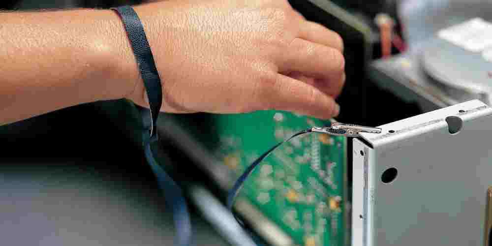
Assembly and Testing
The final step in manufacturing a 5G circuit board is to assemble and test the board. The assembly process involves placing the components onto the PCB using automated or manual techniques, and soldering them onto the board. Once the board is assembled, it must be tested to ensure that it meets the required specifications for performance and reliability. Testing can include functional testing, environmental testing, and electrical testing.
In conclusion, the manufacturing and assembly of 5G circuit boards is a complex process that requires careful attention to detail and a deep understanding of high-speed signal transmission, component selection, and assembly techniques. By following best practices and using high-quality materials and components, manufacturers can produce 5G circuit boards that meet the demanding requirements of next-generation communication systems.
Challenges and Future of 5G Circuit Board Design
Challenges and Limitations of Current Technology
The implementation of 5G technology is a significant challenge for circuit board designers. The high-frequency signals required for 5G communication have a shorter wavelength, which increases the likelihood of signal loss and interference. The current technology used in circuit board design is not optimized for high-frequency signals, which poses a significant challenge to the development of 5G technology.
One of the primary challenges of 5G circuit board design is the need for high-density interconnects. The increased number of components required for 5G technology results in a more complex circuit board design, which can lead to signal loss and interference. The current technology used in circuit board design does not provide the necessary density to support the high-frequency signals required for 5G communication.
Emerging Trends and Future Developments
To overcome the challenges of 5G circuit board design, emerging trends and future developments are being explored. One of the most promising trends is the use of advanced materials. Advanced materials, such as ceramics and polymers, have been shown to provide better signal integrity and reduced signal loss, which is essential for 5G communication.
Another emerging trend in 5G circuit board design is the use of advanced manufacturing techniques. The use of additive manufacturing, such as 3D printing, allows for the creation of complex circuit board designs that are optimized for high-frequency signals. This technology can also reduce the time and cost of circuit board production, making it more accessible for companies to develop 5G technology.
In conclusion, the development of 5G technology presents significant challenges for circuit board designers. The current technology used in circuit board design is not optimized for high-frequency signals, which poses a significant challenge to the development of 5G technology. However, emerging trends and future developments, such as the use of advanced materials and advanced manufacturing techniques, show promise in overcoming these challenges and advancing the development of 5G technology.
