In the process of designing printed circuit boards, PCB layout is a crucial step. Putting parts, traces, and other components on a PCB and assembling them into a functional circuit is complex. Therefore, PCB layout is vital since it can save costs and design time while increasing a circuit’s performance, dependability, and space efficiency.
When developing a PCB layout, manufacturers need to consider numerous factors, including board constraints, manufacturing processes, materials, components, orientation, and organization. The PCB layout procedure additionally entails transforming the schematic into a PCB layout, positioning and rotating components, altering the board’s size and shape, developing a user interface, and adding PCB layers, ground layers, layer thickness, PCB traces, and trace width. This article has provided a comprehensive overview of the process of PCB layout, as well as the benefits of using it. As a result, designers can create more efficient, reliable, and cost-effective boards with a detailed understanding of the PCB layout and its workings.
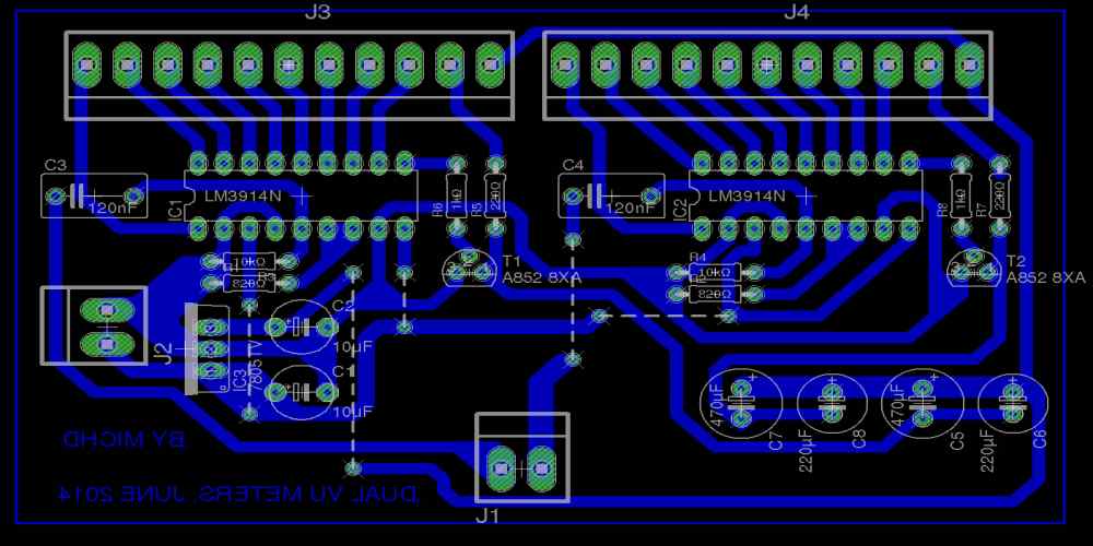
PCB layout
PCB layout is the process of placing electronic components, traces, and other elements on a printed circuit board to form a helpful circuit. By maintaining the size and shape restrictions of the board, the layout maximizes the performance and dependability of the circuit.
PCB layout design considerations, including
1. Board restrictions
The board restrictions set the boundaries for what a particular board design can accomplish. These limits occur due to the size and shape of the board, the materials utilized, and the components that the manufacturers will install on the board. For example, the number of layers, size, routing density, and component spacing are some limitations, though they will vary based on the type of board.
2. Manufacturing Methods
The procedures and steps utilized to make a printed circuit board are known as manufacturing processes. Surface mount technology (SMT), through-hole technology (THT), and flexible printed circuit boards are the most used techniques (FPC). It is vital to consider which approach is ideal for the board design because each has unique requirements and constraints. The most typical method for contemporary PCBs is surface mount technology, which helps mount components to the board.
First, the board is covered with components, which manufacturers subsequently solder to the board surface. This procedure is rapid and efficient, and valuable for most current PCBs. Through-hole technology helps to attach components to the board. However, instead of soldering, components are put through holes in the board and then soldered to the board. This approach is more labor-intensive than surface mount technology but is more reliable for more extensive and heavier components. Flexible printed circuit boards are helpful in applications where the board needs to bend or twist and consists of flexible materials. Applications for this method include wearable electronics and medical equipment.
3. Materials and Components
The materials and components utilized in a board design are essential factors. The materials will affect the board’s strength, flexibility, and electrical qualities. Typical materials used for boards include FR4, FR5, and polyimide. The components will affect the board’s functioning and must be chosen based on the application. Standard components include resistors, capacitors, transistors, and integrated circuits.
4. Component Placement Order
The order designers arrange the components on the board is crucial, as it might affect the board’s functionality. Additionally, the designers should position the components in an order that makes the most sense for the board’s functioning and minimizes the wiring necessary. Typically, manufacturers should set the components to help in the board’s circuit.
5. Orientation
The orientation of components is also significant, as it might affect the board’s functionality. The designers should position the Components in a direction that makes sense for the board’s functioning, and that reduces the amount of wire necessary. Typically, components should be arranged in the same orientation as utilized in the board’s circuit.
6. Placement
The arrangement of components on the board is significant, as it might affect the board’s functionality. Therefore, the manufacturers should place the components in a method that makes the most sense for the board’s functioning and that reduces the amount of wire necessary. Typically, components should be put as close to each other as possible and placed in a way that allows quick access and reworks.
7. Organization
The organization is the placement of components on the board. Position the components in a manner that makes the most sense for the board’s functioning and reduces the amount of wire necessary. Typically, we should set the components in a logical and organized manner, with similar components grouped and with power and ground lines routed in an orderly manner.
What to consider before going for PCB Layout

- Component orientation:
To make your circuit much more straightforward to set up, test, and examine by your manufacturer, you should always place comparable components, such as a group of resistors or LEDs, facing the same direction when positioning them on the board.
- The placing of Components:
Always arrange smaller components in front of bigger ones to ensure a successful soldering procedure. Because taller components would obstruct smaller ones, designers should place them in front since there is a potential that the board you receive will have improperly linked solder joints.
- Routing:
Many inexperienced designers make the error of cramming components too closely together on the board, leaving no room for routing. Because of this, you should always allow enough space between portions so that routing is simple.
PCB Layout Process
1. Converting the Schematic into a PCB Layout
Engineers must transform the schematic into a PCB layout as the first stage in the PCB layout process. This conversion entails taking the schematic design and laying the circuit on a printed board. Designers can accomplish this by arranging the board’s components to connect effectively and take up the least room. Following the placement of the components, the layout is attached using traces, which are conductive lines that link the components and supply the electrical signals required for the circuit to operate.
2. Placing and Rotating Your Components
The designer must utilize a CAD (computer-aided design) tool to position and rotate components on a PCB layout. With the help of this tool, the designer can position components on the board, move them about, and turn them to meet the intended arrangement. The designer can also label the components to make the design more comprehensible and ordered.
3. Resizing the Shape of your PCB
The designer can modify the board’s shape to accommodate the components once they insert and convert them. This action entails altering the board’s size and including cut-outs in the appropriate places. By doing so, designers can customize the board to the desired layout, and the components will fit correctly.
4. The user interface
Making a user interface is the last step in the PCB layout process. This step allows the user to interact with the board and its elements. Many methods, such as a graphical user interface (GUI) or a collection of user-friendly instructions, can help accomplish this. Furthermore, manufacturers can create the user interface so that it is simple to use and that the user can access all of the board’s components and features.
5. PCB Layers:
The PCB (Printed Circuit Board) layout procedure is crucial in the electronics design process. It entails the positioning of parts, the routing of electrical connections, and the development of a circuit board design that can be produced and applied in several ways. Schematic capture, which involves putting all components, nets, and electrical connections into a CAD (Computer Assisted Design) application like Altium Designer, is the first step in the PCB designing process. The designer can start designing the PCB once all the components and connections have been entered.
6. Ground Layers:
FR4, which has a thin copper-coated coating, is one copper-clad material that generally makes up a PCB. The copper layers provide electrical communication between the board’s components. Signal, power, and ground layers are the three primary divisions of the layers. Electrical signals are routed from one component to another using signal layers. Power is distributed to the board’s components using the power layers. The ground layers serve as a point of reference for the electrical signals and are employed to lessen electrical interference and noise.
7. Layer Thickness
A PCB’s copper layers might be anywhere from 1oz and 8oz thick. Naturally, the board will be more conductible the higher the copper thickness. In addition, the thicker copper layers make more routing choices possible, which is advantageous for intricate designs.
8. PCB Traces
The traces on the board make the electrical connections between the components on a PCB. Therefore, the traces must be routed to prevent any potential interference and must be large enough to carry the current required to power the components.
9. Trace Width
The quantity of electricity that must pass through a PCB’s traces is directly proportional to its width. Therefore, a trace may carry more current the wider it is. However, thinner traces are more prone to interference; therefore, designers should determine the trace width based on the noise level the board will be subjected.
Creating PCB Design

- Drawing the Schematic
To produce a PCB design, the designer must draw the schematic. The manufacturers can accomplish this by using a schematic editing program like Altium Designer, KiCad, or Autodesk Eagle. The schematic editor lets the designer depict the circuit’s components, connections, and operation. The designer must define the components as symbols with lines indicating links connecting them and ensure the circuit functions as planned by verifying accurate references.
- Placing Components
After producing the schematic, the designer must arrange the PCB components. To accomplish this, the engineers should use an editor for PCB layout, such as Altium Designer, KiCad, or Autodesk Eagle. The designer is responsible for selecting the locations of the components on the board and ensuring their proper orientation. To avoid poor electrical performance or even electrical shorts, the designer must ensure that the components do not interact with one another.
- Routing
Once the components are in place, the designer must route the copper traces that will connect them. This process involves selecting the correct trace width based on the desired current capacity and manually routing the trace using the mouse. The designer must be careful to avoid crossing or overlapping the traces, as this could result in subpar electrical performance or even electrical shorts.
- Run ERC and DRC To Check for Errors
After routing, the designer must perform the Electrical Rule Check (ERC) and the Design Rule Check (DRC). The ERC reviews the schematic for mistakes, such as faulty connections or misvalued components, while the DRC looks for errors in the PCB layout, such as improper traces or misplaced components. The designer must rectify any mistakes before finishing the design.
Benefits of PCB Layout
- Improved Performance:
A carefully planned PCB layout can enhance a circuit’s performance. In addition, a PCB layout can lessen the impacts of electromagnetic interference, limit signal loss, and lower noise by optimizing the location and routing of components and traces.
- Improved Reliability:
PCB layout can also make a circuit more reliable. A PCB layout can reduce the likelihood of component failure and increase the circuit’s general longevity by ensuring that components are located and routed correctly.
- Space Saving:
PCB layout can assist in reducing the size of a circuit board. A PCB layout can maximize available board space by strategically placing and orienting components and traces, minimizing the need for larger boards or more components.
- Cost Savings:
PCB layout can also assist in cost reduction. For example, a PCB layout can minimize the amount of board space required, the number of raw materials used, and the overall cost of manufacture by optimizing the placement of components and traces.
- Faster Design Time:
A PCB layout can aid designers in finishing their work more quickly and correctly by giving them a visual representation of the circuit and enabling faster and more effective placement and routing of components and traces.
Conclusion
In conclusion, the PCB layout phase of printed circuit board design is crucial. Electronic components, traces, and other components must be arranged on a printed circuit board to construct a functional circuit. The designer must consider the board restrictions, manufacturing methods, materials and details, component placement order, orientation, positioning, and organization during the layout design process. With these factors in mind, designers may build more effective, trustworthy, and cost-efficient boards. Remember that location, orientation, and routing of components are crucial design concerns. By having a comprehensive understanding of the PCB design process, designers of circuit boards may build high-quality boards that meet the specifications of their intended uses.
