When it comes to designing a printed circuit board (PCB), simplicity is often the key. A simple PCB design can be more reliable and cost-effective than a complex one, making it a popular choice for many electronic devices. In this article, we will explore the basics of simple PCB design and how it can benefit your electronic projects.
At its core, a simple PCB design involves minimizing the number of components and connections on the board. This can be achieved through careful planning and layout, as well as selecting the right components for the job. By reducing the complexity of the circuit, you can improve reliability and reduce the risk of errors or malfunctions. Additionally, a simple design can make it easier to troubleshoot and repair the circuit if something does go wrong.
Overall, a simple PCB design can offer many benefits for your electronic projects. Whether you are designing a simple circuit for a hobby project or a complex system for a commercial application, taking a simplified approach can help you achieve your goals more effectively. In the following sections, we will explore some of the key principles of simple PCB design and how you can apply them to your own projects.
Basics of PCB Design
What is a PCB?
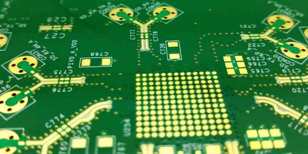
A Printed Circuit Board (PCB) is a board made of insulating material that supports and connects electronic components. It provides a platform for the components to be mounted and connected in a specific layout to form a functional circuit.
Why is PCB Design Important?
PCB design is important because it determines the performance, reliability, and manufacturability of a circuit. A well-designed PCB ensures that the circuit operates as intended, minimizing noise, interference, and other issues that can affect its performance. It also ensures that the circuit can be manufactured efficiently and cost-effectively.
Components of a Simple PCB Design Circuit
A simple PCB design circuit consists of the following components:
-
Components: These are the electronic parts that make up the circuit, such as resistors, capacitors, and transistors.
-
Traces: These are the conductive pathways that connect the components on the PCB. They are made of copper and are etched onto the surface of the board.
-
Pads: These are the metal-plated holes on the PCB where the components are mounted and soldered.
-
Silkscreen: This is the layer of ink on the PCB that provides text and graphics to indicate the placement of components, the orientation of the board, and other important information.
-
Solder Mask: This is the layer of polymer that covers the PCB, except for the pads and traces. It protects the board from damage during soldering and assembly.
In conclusion, understanding the basics of PCB design is essential for creating functional, reliable, and manufacturable circuits. A well-designed PCB ensures that the circuit operates as intended, minimizing noise, interference, and other issues that can affect its performance. By following these guidelines, you can create a simple PCB design circuit that meets your needs and performs to your expectations.
Designing a Simple PCB Circuit

Selecting a PCB Design Software
Before designing a simple PCB circuit, it is important to select the right PCB design software. There are many free and paid options available in the market, each with its own set of features and limitations. Some popular options include Eagle PCB, KiCAD, Altium Designer, and CircuitMaker.
When selecting a PCB design software, it is important to consider factors such as ease of use, compatibility with your computer operating system, and the ability to import and export different file formats.
Creating the Schematic Diagram
Once you have selected the PCB design software, the next step is to create the schematic diagram. This is the blueprint of your circuit and will help you visualize the connections between different components.
When creating the schematic diagram, it is important to follow standard electronic symbols and conventions. You can also use libraries provided by the PCB design software to quickly add components to your circuit.
Layout Design
After creating the schematic diagram, the next step is to design the layout of your PCB. This involves placing the components on the board and arranging them in a way that optimizes the circuit’s performance.
When designing the layout, it is important to consider factors such as component placement, trace routing, and ground planes. You can also use auto-routing tools provided by the PCB design software to automatically connect the components.
Routing
The final step in designing a simple PCB circuit is routing. This involves connecting the components on the board using traces and vias.
When routing, it is important to follow design rules such as minimum trace width, clearance, and via size. You can also use the design rule check feature provided by the PCB design software to ensure that your design meets the required specifications.
In conclusion, designing a simple PCB circuit requires careful planning and attention to detail. By selecting the right PCB design software, creating a schematic diagram, designing the layout, and routing the components, you can create a functional and reliable circuit.
PCB Fabrication

Generating Gerber Files
Before you can manufacture your PCB, you need to generate Gerber files. These files contain all the necessary information about the PCB, including the layout, drill holes, and copper traces. You can use a PCB design software to generate these files. Once the files are generated, you can send them to a PCB manufacturer for fabrication.
Choosing a PCB Manufacturer
Choosing the right PCB manufacturer is crucial for the success of your project. You should look for a manufacturer that can provide high-quality PCBs at a reasonable cost. You can also consider factors such as turnaround time, minimum order quantity, and customer support.
Here are some popular PCB manufacturers:
PCB Assembly
After the PCBs are fabricated, you need to assemble the components onto the board. You can either do it yourself or outsource it to a PCB assembly service. If you choose to do it yourself, you will need to have the necessary tools and equipment, such as a soldering iron, flux, and solder wire. If you outsource it, you should look for a reliable and experienced assembly service.
In summary, generating Gerber files, choosing a PCB manufacturer, and PCB assembly are important steps in the PCB fabrication process. By following these steps, you can ensure that your PCB is fabricated correctly and efficiently.
Testing and Troubleshooting

Testing the PCB Circuit
After completing the PCB design, it is important to test the circuit to ensure that it functions as expected. The following steps can be taken to test the circuit:
-
Check the power supply: Ensure that the power supply is connected correctly and that the voltage is within the range specified in the design.
-
Check the components: Verify that all the components are correctly placed and soldered in the PCB. Check for any shorts or open circuits.
-
Check the signal flow: Use a multimeter and oscilloscope to check the signal flow in the circuit. Verify that the signals are flowing as expected.
Common PCB Design Issues
There are some common issues that can be encountered during the PCB design process. These issues include:
-
Noise: Noise can be introduced into the circuit due to poor grounding, component placement, or routing.
-
Crosstalk: Crosstalk occurs when signals from one trace interfere with signals in another trace. This can be avoided by proper spacing and routing.
-
Thermal issues: High power components can generate heat which can affect the performance of the circuit. Adequate thermal management should be implemented.
Troubleshooting Tips
Even with careful design and testing, issues can arise in the circuit. The following tips can help troubleshoot the circuit:
-
Start with the basics: Check the power supply and components to ensure that they are functioning correctly.
-
Check the signal flow: Use a multimeter and oscilloscope to check the signal flow in the circuit. Verify that the signals are flowing as expected.
-
Use a logic analyzer: A logic analyzer can help identify issues with digital signals.
-
Use a thermal camera: A thermal camera can help identify thermal issues in the circuit.
By following these testing and troubleshooting tips, you can ensure that your PCB design functions as expected.
