The design method known as “via in pad” involves inserting a via inside a component’s copper landing pads. via in pad enables a design to utilize pitch sizes of smaller component as well as further minimize the PCB’s total size when compared to normal PCB through routing.
The hardware engineers are increasingly using via pad techniques due to component manufacturers’ annual push for the smaller parts and consumer desire for smaller gadgets. This article will go over the distinctions between via in pads and conventional vias, when to use them, and how you should build for them.
What Does via in pad Mean?
Via pad represents a printed circuit board design technology that increases filled via PCB density and permits higher circuit board component density (especially in the BGA and SMT IC region) when it applies to circuit design or circuit board fabrication. Additionally, the PCB construction leaves the via pad that the via’s annular ring has been exposed with HAL (like the components exposed by the pad) untreated.
However, as BGA via in pad packages get smaller, via in pads are becoming more common. Altium tented vias could be directly drilled in the BGA footprint pads rather than utilizing the conventional “dog bone” pattern of land to transmit signal across the BGA footprint into a via which carries signal across other layers. By soldering straight over this via, this makes routing considerably simpler.
Ensure that this procedure is noted in your notes. Typically, via in pad can be employed to test the signal, however it can easily cause a short.
What distinguishes Via in Pad from Traditional Vias
The signal can be routed from the pads then to via in conventional vias. In order to prevent the wicking of the solder paste in the via throughout the process of reflow, soldermask can then be applied. This avoids a scenario where there might not be enough solder, leading to a failed connection between the pad as well as the component. This via drill hole is within the pad when the via lies in the pad. As a result, a soldermask cannot be used to tent this via.
Leaving your via open will lead to reliability issues during production if the paste is allowed to wick inside the barrel.
When can you use the Via in Pad?
Using conventional routing techniques to escape and route component packages having a sub pitch of 0.5mm will result in Design Rule Limitations on drill size, annular ring, and trace width should be checked. Traditional PCB techniques for fabrication cannot be used to create smaller, compact traces due to manufacturing constraints on the size of the trace. The only practical approach to route these fine pitch components is with a via in pad that is capped since it enables the routing of the circuit board to remain as small as feasible.
Thermal pads’ vias can also aid in controlling heat. The thermal pad which mounts onto the filled via PCB is generally present on surface mount components of high power. It is good to drop the altium tented vias through a circuit board to the PCB’s other side to expand the area of the copper for the release of heat in order to dissipate this heat better.
Thermal pad vials may have an impact on how heat is managed. Surface mount components of high power typically have thermal pads which attaches to circuit boards. To expand this area of copper for the release of heat, you should drop the vias through that circuit board into the opposite side of your PCB.
Why not then use a via in pad on every via? Increased manufacturing material and complexity costs of the fabrication process of the PCB outweigh the benefit of reduced component fan outs as well as routing complexity. If you can achieve your hardware design using the traditional style through routing, you are advised to avoid using the via in pad.
Design Process for the Via in Pad
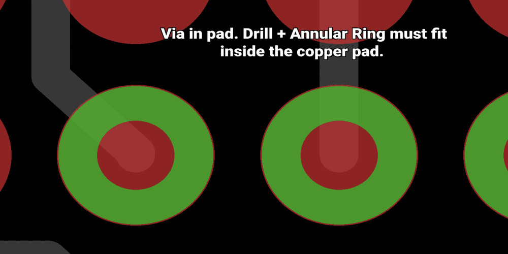
Via in pad implementation is similar to vias in general. The way it affects your PCB design rule check as well as how these files for manufacturing are made differs. Ensure that the via in pad satisfies the least annular ring criteria specified by the manufacturer. This minimum size for the annular ring must be met, or it must be exceeded, by the component footprint’s pad size.
Typically, this isn’t a problem because most pad sizes were bigger than through sizes, but like BGA via in pad packages go smaller; this can become the design challenge. Utilizing Solder Mask pads that will be the best choice if the BGA’s landing pad diameter is smaller compared to the sum of the via as well as annular ring diameters.
Via In Pad PCB

With PCB design, the via refers to a pad containing a tiny plated hole that connects copper tracks across different levels of the board. For the high density multilayered PCBs, there’s a via referred to as micro via that only has visible blind vias on a single surface or the invisible buried vias across both surfaces.
In addition, the introduction and widespread use of pin out part of high density, in addition to the requirement for compact dimension PCB, have created a new problem. Consequently, adopting the most recent but well-liked PCB manufacturing tech known as “via in pad” is the superior way to handle this type of issues.
Due to the necessity to minimize the form factor of the PCB and the ongoing reduction in component footprint pitch, it is urgently necessary to use via in pads in the present via in PCB design. Additionally, it may achieve the signal routing in the smallest possible area within the PCB layout, frequently even avoiding fleeing the device footprint’s boundary.
When Should PCB Designers Use Via in Pad?
Is each PCB layout acceptable for the via in pad design? It’s crucial to think about whether the subsequent requirements apply to your individual design before implementing a via in pad.
Enhanced Density
Via-in-pad design can help you conserve PCB space whenever you must squeeze a lot of traces and components into a tiny space by minimizing the amount of vias present on the board’s surface.
Enhancement of Thermal Performance
The via in pad design offers a direct heat path into the copper plane, which can aid in transferring heat from the heat-generation components like power devices.
Enhancing Electrical Performance
Via in pad can create low-impedance connections between the components as well as inner circuit board layers whenever you want to enhance the circuit’s electrical performance.
Applications for High-Frequency
Via in pad may prove helpful for the high-frequency applications to improve signal integrity and control connection impedance.
Via-in-pad can however have certain disadvantages, including potential temperature stress on the components, the higher cost, as well as more complex production requirements. Overall, the circuit board’s unique requirements and limitations determine whether a via in pad design is appropriate.
Via in Pad Applications
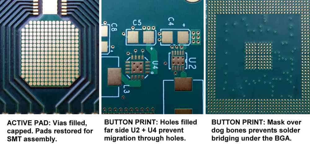
When creating PCBs whenever there isn’t sufficient space for typical vias, PCB designers employ vias in pads. Since there isn’t enough capacity for additional vias in the BGA package, they are frequently used with those components in that package.
Small-sized SMD components with a lot of pins were permanently fixed using BGA packages. Every single pin of the components within BGA packaging is methodically organized into a matrix and has a little solder ball on it. Unlike other frequently used packages like dual-in-line (DIL) packages, the BGAs provide ruggedness and greater packing efficiency.
Surface routing can be quite difficult in BGAs since the solder balls’ sizes and the space between surrounding pins might be as thin as a mere fraction of the millimeter. Every pin might have a track created that leads it to a location where a via could be made with very narrow trace width. However, it’s not the best strategy.
Circuit board design software would issue warnings for components whose pin spacing is less compared to the clearance’s safe track.
To take this signal carried through the pins of component into the necessary PCB layers, the vias may be built directly below the BGA pads as a substitute to attempting to route the pins away while constructing a via distant from that component.
What Benefits does Via in Pad routing offer?
The following are some advantages of via in pad for board design:
Saves space
One among the main justifications for employing via in pads is space conservation,. Vias in pads are formed directly on the pads of the components, conserving space, as opposed to conventional vias that need the routing of the signal away from these pad. By doing away with the need to create dog-bone tracks, these improve routing and significantly lower the total PCB footprint.
Simpler routing
Allowing vias to be placed just beneath the pad doesn’t just free up space; it also simplifies routing (particularly for components with small footprints, like those found in BGA packages).
Better heat dissipation
The via in pads may significantly boost heat dissipation for heat sources located on the printed circuit board which will result in better cooling. This thermal conductivity in-between these components as well as the various layers of a PCB is improved when a through is placed close to the heat source, enabling faster heat dissipation.
Vias in pads additionally reduces parasitic inductance related to them since they do away with the extra connecting segment. Bypass capacitors can be placed adjacent to the components thanks to vias in the pads, which reduce inductance. This leads to better signal integrity for the high-speed interfaces and designs.
The Drawbacks of Via in Pad
To make a great design choice, users of via in pads must be aware of a few drawbacks. Before deciding on a via in pad design, PCB designers should always have a look at these considerations.
A higher cost of production: More than simply hole drilling and covering it with a layer of conductive material is frequently needed to create vias in pads. To boost the pad’s mechanical strength, vias must be filled using conductive epoxy or any other type of conductive fillers. As a result, the process of PCB assembly requires more steps and has higher material prices. The accompanying expenses are further increased by the idea that costs of producing vias in pads don’t scale down linearly with a rise in the quantity of the manufactured units.
Surface ridges: When these vias aren’t positioned and filled exactly, surface bumps develop. These surface flaws can make the situation more difficult.
Therefore, producers must guarantee that all surface roughness are removed before forming vias in pads. Vias in pads are challenging to design as well as install, which increases design complexity.
Via in Pad vs Conventional Vias PCB Design
Although functionally, implementing the vias in pad is fairly similar to applying traditional vias, there are some important considerations that designers have to consider while working on PCB manufacturing and design. As follows:
Verifying the design capabilities of a PCB manufacturer: The abilities of the production process are described on websites for PCB makers. To prevent DRC and DFM issues, designers must first visit the website of the manufacturer to understand various characteristics including the minimal size of the annular ring.
removing every necessary file from your circuit board design tool: Many misunderstandings and problems can be resolved by carefully analyzing the designs following exporting from EDA tools. By providing an additional file with a map of only the vias in pads as well as to the file with a map of drills, it is ensured that conventional vias won’t be filled or capped
Conclusion
Electrical signals are transferred between the various layers of the multi-layer PCBs using vias. Vias may be constructed directly on the pads rather than routing the signal from the pin and establishing a conventional via. Making vias in pads reduces the parasitic inductance while also saving space, streamlining routing, and improving thermal management. Generally speaking, vias in pads cost more than standard vias. To ensure the boards are made without difficulty, designers must confirm the PCB manufacturer’s design capabilities and make sure all necessary files are removed from the printed circuit board design program.
