PCB design and assembly are two critical steps in the process of creating electronic devices. PCBs, or printed circuit boards, are the foundation of most electronic devices, providing the necessary connections between electronic components. The design and assembly of these boards require careful planning and execution to ensure that the final product meets the desired specifications.
The design process involves creating a schematic of the circuit and laying out the components on the board. This is a complex process that requires knowledge of electrical engineering, as well as specialized software tools. Once the design is complete, the board must be manufactured, which involves etching the board and adding the necessary layers of copper and other materials. The assembly process involves placing the components on the board and soldering them in place. This is a delicate process that requires precision and attention to detail to ensure that all components are properly connected and the board functions correctly.
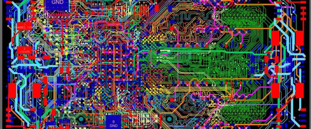
PCB Design
When it comes to designing a printed circuit board (PCB), there are several steps involved. These include schematic capture, layout design, and design rule check. Let’s take a closer look at each of these steps.
Schematic Capture
The first step in PCB design is schematic capture. This involves creating a visual representation of the circuit you want to build. This can be done using software such as Altium Designer or Eagle PCB. The schematic should include all the components you plan to use, as well as the connections between them. It’s important to ensure that the schematic is accurate and complete before moving on to the next step.
Layout Design
Once you have a completed schematic, the next step is layout design. This involves placing the components on the PCB and routing the connections between them. It’s important to consider factors such as component placement, signal integrity, and thermal management when designing the layout. You can use software such as KiCad or OrCAD to create the layout. It’s important to note that the layout should be optimized for manufacturability, as this will make the assembly process smoother.
Design Rule Check
Before sending your design to be manufactured, it’s important to perform a design rule check (DRC). This involves checking your design against a set of rules that ensure it meets the requirements for manufacturability. These rules can include things like minimum trace width and spacing, minimum drill size, and clearance between components. You can use software such as CAM350 or BluePrint to perform the DRC. It’s important to fix any errors that are found before sending your design to be manufactured.
In conclusion, designing a PCB involves several steps, including schematic capture, layout design, and design rule check. It’s important to ensure that each step is completed accurately and thoroughly in order to create a functional and manufacturable PCB.
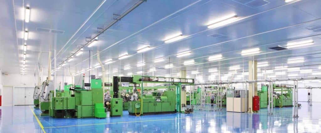
PCB Assembly

PCB assembly is the process of attaching electronic components to a printed circuit board (PCB). This process involves several steps, including component placement, soldering, and testing.
Component Placement
Component placement is a critical step in the PCB assembly process. It involves placing electronic components on the PCB in their correct positions. This process can be done manually or using automated equipment.
Manual component placement requires a skilled technician who can accurately place the components on the PCB. Automated equipment, on the other hand, uses pick-and-place machines that can place components with high accuracy and speed.
Soldering
Soldering is the process of attaching electronic components to the PCB using solder. This process involves heating the solder to a temperature that melts it, allowing it to flow and bond the component to the PCB.
There are several methods of soldering, including wave soldering, reflow soldering, and hand soldering. Each method has its advantages and disadvantages, depending on the complexity and size of the PCB.
Testing
Testing is the final step in the PCB assembly process. It involves checking the PCB for any defects or faults that may have occurred during the assembly process.
There are several methods of testing, including visual inspection, electrical testing, and functional testing. Visual inspection involves checking the PCB for any physical defects, such as missing components or misaligned solder joints. Electrical testing involves checking the electrical properties of the PCB, such as resistance and capacitance. Functional testing involves checking the PCB’s performance by connecting it to a power source and measuring its output.
In conclusion, PCB assembly is a complex process that requires skilled technicians and specialized equipment. Component placement, soldering, and testing are the critical steps in this process. By following these steps carefully, manufacturers can produce high-quality PCBs that meet the requirements of their customers.
PCB Manufacturing
When designing a printed circuit board (PCB), it is essential to understand the manufacturing process. There are three main steps in PCB manufacturing: Gerber file generation, PCB fabrication, and PCB assembly.
Gerber File Generation
Gerber files are the industry-standard format for PCB design. These files contain all the necessary information for the PCB manufacturer to create the board. The Gerber files include the PCB layout, drill holes, and other specifications.
It is crucial to ensure that the Gerber files are accurate and error-free. Any mistakes in the files can result in a faulty PCB. Before sending the files to the manufacturer, it is recommended to double-check them and use a Gerber viewer to verify the design.
PCB Fabrication
Once the Gerber files are generated, the PCB manufacturer will use them to fabricate the board. The fabrication process involves several steps, including printing the design onto a copper-clad board, etching away the unwanted copper, and drilling holes for components and vias.
PCB manufacturers use various techniques to fabricate PCBs, such as chemical etching, milling, and laser cutting. The choice of method depends on the complexity of the design, the number of layers, and the required accuracy.
PCB Assembly
After the PCB is fabricated, the next step is to assemble the components. PCB assembly involves placing the components onto the board and soldering them in place. There are two main methods for PCB assembly: surface mount technology (SMT) and through-hole technology (THT).
SMT components are smaller and lighter than THT components, making them suitable for compact designs. THT components are larger and easier to handle, making them ideal for prototypes and low-volume production.
In conclusion, understanding the PCB manufacturing process is crucial for designing a successful PCB. By following the steps of Gerber file generation, PCB fabrication, and PCB assembly, you can ensure that your PCB is accurate and reliable.
