Custom Printed Circuit Boards (PCBs) have become an integral part of our modern technological world, providing the backbone for a wide variety of electronic devices. From consumer electronics and medical equipment to aerospace and automotive applications, the demand for reliable and specialized PCB design continues to grow. This guide aims to give you the ultimate resource for achieving the best results with your custom PCB designs.
Choosing the right materials, layout techniques, and manufacturing processes can have a significant impact on the performance, longevity, and reliability of your custom PCB. In this guide, we will dive into the essential aspects of PCB design and provide tips and tricks for navigating the world of custom PCB production. By understanding the nuances of this complicated field, you can ultimately save time, reduce costs, and create a more efficient and reliable final product.
As technology continues to advance rapidly, staying informed and up-to-date with the latest trends and techniques in custom PCB design is essential for success. We understand this need and will provide you with the knowledge to make informed decisions, ensuring that your custom PCBs deliver exceptional performance and meet their intended application requirements. Get ready to explore the ins and outs of custom PCB design and learn how to get the best results possible from your projects.
Custom PCB Basics
Types of PCBs
There are several types of printed circuit boards (PCBs) used in various applications. Some common ones include:
- Single-sided PCBs: These have components and connections on one side of the board.
- Double-sided PCBs: These have connections on both sides of the board, allowing for more components and dense circuitry.
- Multi-layer PCBs: These consist of multiple layers of circuitry, allowing for even higher component density and complex designs.
Applications
Custom PCBs have a wide range of applications across various sectors. Some examples include:
- Consumer electronics: Devices like smartphones, laptops, and televisions rely on custom PCBs for efficient functionality.
- Industrial control systems: Custom PCBs are essential in manufacturing equipment and factory automation systems.
- Medical devices: PCBs play a crucial role in medical equipment, from diagnostic devices to medical imaging systems.
Industries
Custom PCBs are utilized across a diverse range of industries. Here are some examples:
- Automotive: Modern cars and electric vehicles incorporate custom PCBs for their control systems, infotainment, and more.
- Aerospace: PCBs are crucial in avionic systems, satellite communication, and space exploration missions.
- Telecommunication: Custom PCBs are used in networking devices, routers, and other communication tools.
Design Considerations
Design Software Options
There are various design software options available for creating custom PCBs. Some popular choices include:
These software tools offer various features and options, so it’s essential to choose a program that suits your needs and experience level.
Design Rules and Constraints
To ensure your PCB functions reliably, follow standard design rules and constraints. These may include:
- Trace width and spacing
- Via size and annular ring size
- Minimum hole size
- Keep out zones
- Component placement constraints
- Copper weight and thickness
Adhering to these guidelines helps in avoiding manufacturing issues and ensuring board functionality.
Layer Stack-up and Material Selection
Selecting the right layer stack-up and materials for your PCB is crucial. Consider factors such as:
- Number of layers: Single-layer, double-layer, or multi-layer PCBs
- Material type: FR-4, Rogers, Teflon, or other specialized materials
- Copper thickness: This affects the current carrying capacity and impedance control
- Dielectric constant: Determines the electrical properties of the insulating material
Proper selection contributes to the PCB’s overall performance and reliability.
Signal Integrity and EMC Compliance
Signal integrity (SI) and electromagnetic compatibility (EMC) are critical aspects of PCB design. Some factors to consider are:
- Impedance matching: Ensure consistent impedance across traces to minimize signal reflections and losses
- Grounding techniques: Proper grounding helps to reduce noise and improve EMC
- Routing guidelines: Adhere to best practices to avoid crosstalk and maintain SI
- Decoupling capacitors: Use appropriate capacitors to stabilize power supply voltages
By considering these factors, you can design a robust and reliable custom PCB.
Manufacturing Process

PCB Fabrication
The PCB fabrication process begins with creating a design of the desired circuit, which is fed into a Computer-Aided Manufacturing (CAM) system. The CAM software verifies and corrects the layout to optimize it for manufacturing. Then, the circuit pattern is transferred onto copper-cladded laminates through etching or other techniques, followed by drilling holes for through-hole components and applying a solder mask to protect the copper traces and prevent short circuits.
The final steps in PCB fabrication involve adding a silkscreen layer for labeling components and a surface finish to prevent oxidation and ensure proper soldering of components. Several popular surface finishes include HASL (Hot Air Solder Leveling), ENIG (Electroless Nickel Immersion Gold), and OSP (Organic Solderability Preservatives). After completing these steps, the bare PCB boards are ready for assembly.
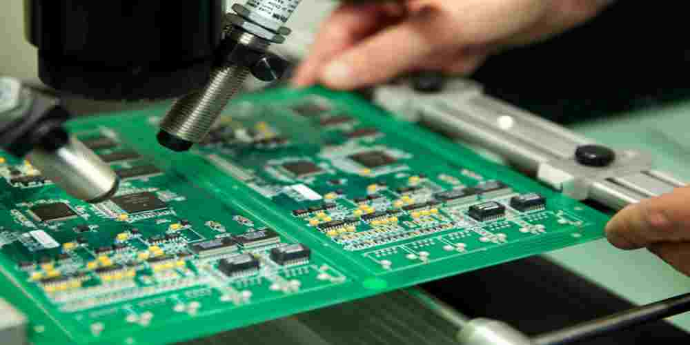
Assembly
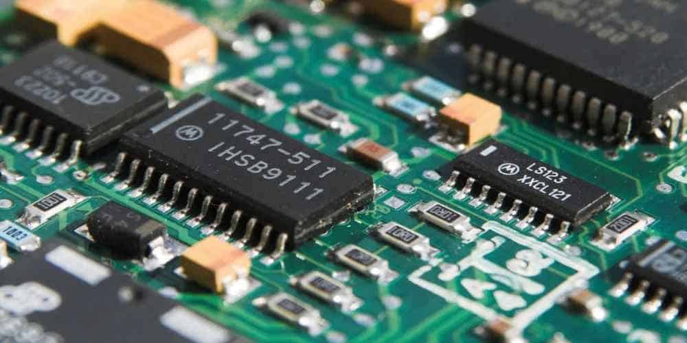
In the assembly stage, components are inserted into the PCB to create a functioning system. There are two types of assembly techniques:
-
Through-Hole Technology (THT): Components with leads are inserted into the pre-drilled holes and soldered to pads on the opposite side of the board. This method is suitable for large components and provides a strong mechanical connection.
-
Surface Mount Technology (SMT): Components are soldered directly to copper pads on the surface of the PCB. SMT components are smaller and can be mounted on both sides of the board, allowing for higher component density.
The assembly process is mainly automated, using pick-and-place machines, which place components onto solder paste, followed by a pass through a reflow soldering oven.
Testing
After assembly, PCBs undergo several tests to ensure their functionality and quality. Some common testing methods include:
-
Visual Inspection: Trained technicians or automated optical inspection (AOI) machines check for soldering defects, misaligned components, and other issues.
-
Functional Testing: Powered up and exposed to specific test scenarios to verify that they are functioning as intended.
-
In-Circuit Testing (ICT): Using a bed-of-nails fixture, an ICT machine measures electrical values, such as resistance, capacitance, and voltage, to detect any defects in the assembled PCB.
By following a rigorous manufacturing process with proper design, fabrication, assembly, and testing, custom PCBs can be produced with high quality and reliable results.
Quality and Reliability
Quality and reliability are crucial factors when considering custom PCBs. This section discusses various inspection techniques, certifications, and standards to ensure the best results.
Inspection Techniques
There are several inspection techniques employed to evaluate the quality of custom PCBs:
- Visual inspection: The simplest and most common method, visual inspections detect any potential issues and surface defects.
- Automated Optical Inspection (AOI): This technique uses cameras and image processing software to identify defects, such as component placement errors and soldering issues.
- X-ray inspection: X-ray inspection is used to examine internal structures and hidden defects, especially for multi-layered PCBs and solder joints.
Certifications
Certifications guarantee that a custom PCB manufacturer adheres to specific quality standards. Some of the common certifications include:
- ISO 9001: An international standard for Quality Management Systems (QMS).
- ISO 13485: Specific to medical devices, this standard ensures that PCBs are designed and manufactured to meet stringent requirements.
- IPC-A-610: Widely followed in the electronics industry, this standard governs the acceptability of electronic assemblies.
Standards
Compliance with industry-standard specifications is paramount in custom PCB manufacturing. Some key standards to consider are:
- IPC-2221: Generic Standard on Printed Board Design.
- IPC-6012: Qualification and Performance Specification for Rigid Printed Boards.
- IPC-A-600: Acceptability of Printed Boards.
By adhering to these inspection techniques, certifications, and standards, custom PCB manufacturers can deliver the highest quality and most reliable products to their customers.
Sourcing Components
Component Selection
When designing a Custom PCB, it is crucial to select components that best suit your project requirements. To achieve the best results:
- Consider the availability of components, ensuring they are easily sourced.
- Compare different manufacturers’ specifications and pricing.
- Take into account the operating conditions and ensure the component’s performance matches your application.
Supply Chain Management
Managing your supply chain is an essential aspect of obtaining components for a Custom PCB. Efficient supply chain management ensures you get components on time and at the lowest cost. Here are a few suggestions:
- Develop strong relationships with suppliers and maintain transparent communication.
- Use a Bill of Materials (BOM) to track and organize your component requirements.
- Monitor lead times and stock levels to avoid delays in production.
Cost Optimization
Design Strategies
To optimize the cost of your custom PCB, several design strategies can be employed. Some effective methods include:
- Component selection: Choose cost-effective, readily available components that meet your project requirements.
- Minimizing board size: Decrease the PCB’s overall dimensions to reduce production costs, as materials and manufacturing labor are charged per unit area.
- Optimizing board layers: Utilize an optimal number of layers, minimizing cost while maintaining necessary design complexity.
- Efficient placement: Strategically place components to minimize the need for additional layers and traces, reducing production costs.
Production Volume Considerations
When looking to optimize costs for your custom PCB project, production volumes must be taken into account. The relationship between production volume and cost can be divided into three categories:
-
Low-Volume Production: For small quantities, the cost per unit will be higher due to setup fees and non-recurring engineering costs. This option is suitable for prototyping or small runs.
-
Medium-Volume Production: As the production volume increases, the cost per unit generally decreases, making this a more cost-effective choice for orders that lie between the low and high volume categories.
-
High-Volume Production: At high production volumes, the cost per unit becomes the lowest. However, this option may require more upfront investment, and changes to the design can be difficult or expensive to implement.
By considering design strategies and production volume, you can optimize the cost of your custom PCB while still achieving the desired results.
After-Sales Support
Maintenance Tips
Regular maintenance of your custom PCB can extend its lifespan and improve performance. Here are some general maintenance tips:
- Clean the PCB regularly using a soft brush or compressed air to remove dust and debris.
- Inspect the solder joints and components for signs of wear or corrosion.
- Store PCBs in a dry, cool place when not in use.
- Avoid exposing the PCB to extreme temperatures or humidity conditions.
Troubleshooting Common Issues
Facing issues with your custom PCB? Here’s a list of common problems and potential solutions:
- Poor Soldering: Inspect the solder joints and reflow if necessary. Use a soldering iron with an appropriate temperature setting.
| Issue | Solution |
|---|---|
| Poor solder adhesion | Clean the PCB and ensure it is free of contaminants |
| Cold solder joints | Increase soldering temperature and time |
| Overheated components | Decrease soldering temperature |
-
Component Failures: Check for damaged or malfunctioning components. Replace faulty components with new ones as needed.
-
Short Circuits: Use a multimeter to identify and locate short circuits. Inspect the board layout for potential shorts.
-
Power Issues: Ensure the power supply is functioning correctly and provides adequate voltage/current to the PCB. Check for damaged components in the power supply circuit.
Remember to always consult the documentation or support resources provided by the PCB manufacturer first when encountering issues.
