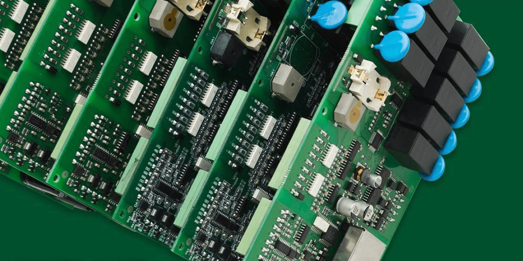
The process of producing the printed circuit boards (PCB manufacturing) is a very complex one. This usually begins from the product concept, which eventually comes to an end with a finalized PCB assembly. All through the process, there is a creation of a schematic which assists in the capture of its net connectivity, electronic components order, as well as the layout of the PCB design’s physical circuitry.
Once you are through with soldering the board’s components, as well as finishing the testing of the PCB assembly and verifying it, then your circuit board thickness will be incorporated into the system.
Also, there are so many important details that takes a printed circuit board all through, from the beginning and then to the final part to make sure of success. One aspect that hardly gets enough notice is the PCB fabrication. So much attention is given to the PCB design which is happening as a result of the software tools usually used, and which play a significant role during the creation.
So what processes does PCB fabrication service involve? Before we go into details, we will discuss the requirements for constructing the best possible PCB fabrication whereby contract manufacturers will be able to assemble with ease.
Important Requirements for PCB Fabrication
Here are some of the important things to put in place before you begin the process of PCB fabrication.
The Circuit Board’s Details
Before you begin with the circuit board layout, then your design team must work hand in hand with your contract manufacturer for developing the parameters as well as configuration of your board. In addition, this is a very useful information for your design layout. This also aids in deciding the best possible vendor to handle your PCB fabrication.
Finalized PCB Design
In order to ensure accuracy in your PCB manufacturing, there is a need to finish your initial design. Also, the updates of a component, which wasn’t synchronized in-between your layout as well as the schematic could result into an altered footprint. This then causes a board build that is faulty.
Complete Data for the Design of PCB Manufacturing
Now this design has now been set, then the next step is building. This stage involves generating some data files for the PCB assembly as well as fabrication. These are now passed to your contract manufacturer.
Once you are through, the contract manufacturer makes use of the files for making these reviews. The next step is to direct them to a fabrication vendor. This fabricator vendor will then give you a quote to build your raw boards.
After completing the checklist items and ready, then your contract manufacturer will be able to continue with how to make orders for your circuit boards which are very important for your pcb assembly.
Explaining the Process of PCB Fabrication

In this section, we’ll be considering the major steps for fabricating a multilayer circuit board (pcb fab).
Circuitry Images Creation
Here, the initial step for fabrication of circuit boards involves the transfer of the image data of the circuitry of the circuit board from your manufacturing files that your contract manufacturer has delivered into the board.
In addition, this data appears in a unique file referred to as the Gerber. Although, you can utilize other formats as well as databases. Making use of any of these methods entails the transfer of its image data onto the circuit board edges.
Direct imaging: Here, the laser prints the images of the circuitry directly onto your circuit board. When it does this, it is able to bypass the usefulness of the photo tools. Also, this is much more beneficial in contrast to the utilization of the film as a result of its extremely precise nature, no alignment problems. In addition, all the outer layers must be laser printed. This causes the whole process to become more expensive.
Photo Tooling: Photo tooling is very useful in the process of PCB fabrication and has been in use since the mass production of circuit boards. In addition, this precision photoplotter ensures the creation of the whole circuitry image found on film, which offers great benefits in the entire process of fabrication to become a very significant template in printing all the images onto the board.
The Layers of the Circuit Board
Multilayer printed circuit boards are composed of layers of a dielectric material as well as metal conductors. In addition, this is composed of some thin layer pairs featuring a dielectric material that involves glass fiber commonly referred to as the epoxy resin and FR4. Furthermore, this is usually sandwiched between the two layers copper foil. Although some dielectric materials are available, the FR4 is well-known as the best frequently used material that serves the process of PCB fabrication.
Also, the core structure of multilayer boards is similar to that used for creating double sided in board. In addition, it helps in laminating it altogether with other structures present in the building of the stackup of its board layer. Every layer has to be controlled strictly for copper weight, layer alignment, as well as width to make sure that the final product is of high quality.
Creating the Circuitry of the Inner Layer
First in the PCB fabrication involves the circuitry images printing into the cores of its inner layer.
- Copper foil present in cores is usually covered making use of a specific photoresist sheet.
- Next, the photoresist becomes exposed using either UV light through direct imaging making use of a specific laser as well as photo tooling.
- Just areas of your copper circuitry i.e. excess copper pads as well as traces are usually exposed. This helps in hardening or polymerizing the photoresist found above the patterns of the copper circuitry. The photoresist left unexposed and pliable is taking out in a chemical way from copper.
- Next, copper layers present in the core become etched away. Now, this will leave the circuitry areas with protection from polymerized photoresist.
- Once the process has been completed, then the layers present in the core would go through AOI inspection for possible defects. Once the inner layer of the circuit board passes through same AOI process, they are ready for lamination in just one circuit board.
Lamination the whole Layers Altogether

To ensure the bonding layers, each of the layer pair has to feature prepreg sheets placed in-between. This prepreg is called fiberglass material, which is usually impregnated with the help of epoxy resin and it melts during heat coupled with pressure from the entire process of lamination. Immediately the cooling of the prepreg takes place, it bonds all the layers.
The board’s composition coupled with other phases requires much attention. In addition, this individual must be detailed so as to maintain proper alignment of this circuitry. The next stage has to do with laminating the whole sandwiched layers. In addition, the pressure, as well as heat process fuses all the layers in a printed circuit.
Drilling of the Holes
The next phase in the PCB fabrication involves holes drilling in the circuit board. This helps with mounting the components, through hole vias, as well as holes that are non-plated having contrasting mechanical features. In addition, a good number of thru-holes are useful for the printed circuit board is all plated.
In addition, the design features laser-drilled microvias as well as blind or buried vias. All these are first fabricated even before the circuit board lamination. These extra steps in the process can lead to more costs during the fabrication. Moreover, they may be very important for a dense circuitry as well as electrical performance.
One through with the hole drilling process, these are cleaned utilizing different chemical as well as mechanical processes so as to take out debris coupled with any resin smears present from the drilling.
Creating the Bottom as well as the top layer Circuitry
Here, this circuit board is then ready to accept the printing of its bottom as well as top images of the circuitry. To make this possible, the photoresist is utilized within its inner layers. Moreover, the time, all the circuitry won’t require any form of protection. Also, it must be plated utilizing more copper.
- First step is the full covering of the top, inner as well as bottom surfaces using the photoresist material. It will involve the holes that are drilled requiring plating.
- Exposing the photoresist can be done by laser as well as UV. Moreover, the whole surface layers of the circuit board will become exposed apart from the patterns of the circuitry.
- Once the chemical cleaning of the photoresist left unexposed has been done, the bare copper’s circuitry patterns will then be electrically plated. This will assist with the building up of the metal’s weight
- Next involves the plating of the entire copper circuitry. Now, this serves as its protective layer. In addition, the photoresist gets removed from the circuit board remaining to get prepared for etching.
- The next step involves the board etching. This aids in removing copper. This excludes metal circuitry regions, which are well-protected with the help of the tin.
- Finally, this involves taking out the tin and leaving behind the thru-holes, copper pads, As well as the traces
As at now, you have completed the military board circuitry. Moreover, there are some important steps that aid in completing the circuit board fabrication.
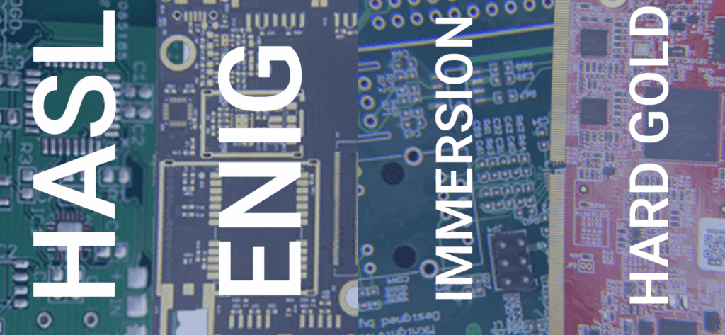
The Surface Finishes, Silkscreen, as well as Solder Mask
To safeguard the circuit board during an assembly, then you have to apply the material of solder mask utilizing UV exposure. Furthermore, this shares some similarities to that used when the photoresist is on. That solder mask helps in covering the surface of your circuit board asides the features as well as metal pads which needs soldering.
In addition, asides solder mask, its reference designators coupled with the marking on the board will then undergo the Silkscreening process onto the circuit board. Furthermore, the silkscreen, as well as the ink of the solder mask will become cured. This has become possible via the oven baking of that particular circuit board.
Furthermore, this board includes a specific surface finish that is applied to metal surfaces that are exposed. When this happens, this provides adequate protection to the metal left exposed. In addition, it helps the soldering process to the completion of the assembly.
The first step includes the coating of the board making use of flux. This prepares it for use by the solder, then it becomes dipped in the bath of the molten solder. Once you are taking the board out of the solder board, there is a hot air blast that assists in taking out too much solder paste inside all the holes. After doing this, it goes ahead to smoothen out the solder mask available on its surface metal.
Inspection, the Assembly Preparation as well as Testing
This is the final of the entire process involved in PCB fabrication. This has to do with preparing the board to undergo assembling. Furthermore, if required, the circuits become routed from the panels. Also, the preparation of the panels can be done for the breakout once the assembly is completed. This is achievable through the routing out of the board.
Then, the finished product will be made to pass through some continuity testing utilizing automated equipment for testing. Furthermore, tests seek some unintentional shorts found in nets that may have led to the board’s invalidation. Once done with the testing process, and this board passes all the necessary inspections, then it gets shipped to your CM to begin the component procurement and assembly of the components.
Conclusion
The circuit board or process of PCB fabrication might be a very easy as well as direct process in the pcb industry. Moreover, you have to put some other things in the right place before you go ahead. Furthermore, to make sure of circuit boards or rigid flex boards with great quality, there is a need to take a look at some features even before you choose a company or pcb vendor to handle your prototype PCBs and PCB fabrication.
