Gerber design is a crucial aspect of printed circuit board (PCB) manufacturing. It involves the creation of a set of instructions that guide the fabrication process of a PCB. These instructions are generated in a standard file format known as Gerber files. The Gerber design process is a critical step in ensuring that the final product meets the required specifications.
Gerber files contain information about the PCB’s layout, including the placement of components and the routing of traces. The files are used by manufacturers to create a photomask, which is used to transfer the design onto the PCB substrate. The Gerber design process involves the use of specialized software that allows designers to create and edit the layout of a PCB. It is essential to ensure that the design is error-free and meets the required specifications to avoid costly errors during the manufacturing process.
In conclusion, Gerber design is a critical step in the manufacture of printed circuit boards. It involves the creation of a set of instructions that guide the manufacturing process and ensure that the final product meets the required specifications. The Gerber design process is a complex and highly specialized field that requires expertise and attention to detail.
What is Gerber Design PCB?
Gerber Design PCB is a file format used in the manufacturing of printed circuit boards (PCBs). It is a standard format for the transfer of PCB design data from design software to the fabrication process. The Gerber format was first developed by Gerber Scientific Instruments in the 1960s, and it has become the industry standard for PCB fabrication.
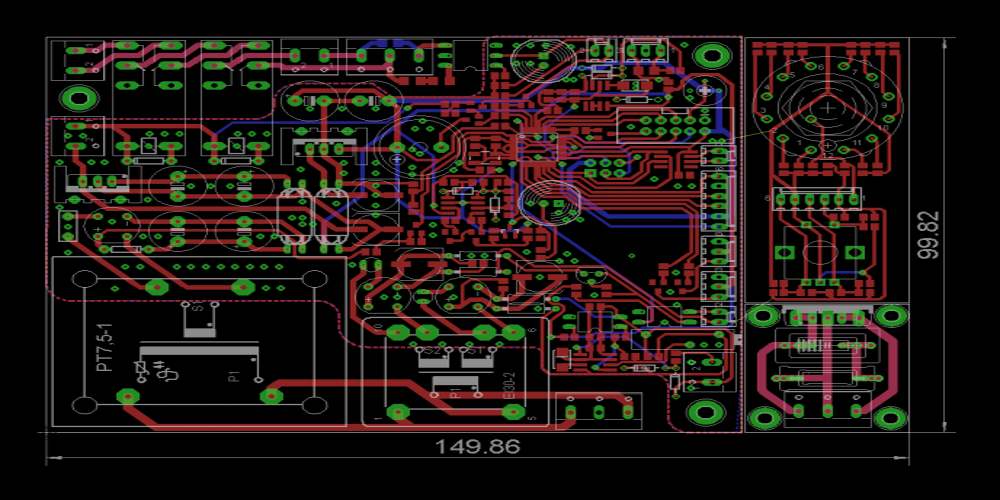
The Gerber Design PCB format consists of a set of files that describe the various layers of the PCB, including the copper traces, solder mask, and silkscreen. The files are generated by the PCB design software and are then sent to the PCB manufacturer for use in the manufacturing process.
One of the benefits of using the Gerber Design PCB format is that it allows for a high degree of accuracy in the manufacturing process. The files are designed to be read by computer-controlled machines, which can precisely replicate the design on the PCB. This results in a high-quality, reliable PCB that meets the exact specifications of the design.
In addition to its accuracy, the Gerber Design PCB format is also widely supported by PCB manufacturers and design software vendors. This makes it easy to find a manufacturer who can produce a PCB from a Gerber file, and it also ensures that designers can use the software of their choice to create the design.
Overall, the Gerber Design PCB format is an essential tool for PCB designers and manufacturers. It provides a reliable, accurate, and widely supported method for transferring design data from software to the manufacturing process.
Advantages of Using Gerber Design PCB
Gerber design PCB is a popular choice for designing printed circuit boards (PCBs) due to its numerous advantages. Here are some of the key benefits of using Gerber design PCBs:
-
Accuracy: Gerber design PCBs are highly accurate, ensuring that the final product matches the design specifications. This reduces the likelihood of errors and saves time and money in the long run.
-
Flexibility: Gerber design PCBs are highly flexible, making them suitable for a wide range of applications. They can be used to create complex designs, and can be customized to meet specific requirements.
-
Ease of use: Gerber design PCBs are easy to use, even for those with little or no experience in PCB design. This is because they are supported by a wide range of software tools that make the design process simple and intuitive.
-
Cost-effective: Gerber design PCBs are cost-effective, making them a popular choice for both hobbyists and professionals. They are also widely available, which helps to keep costs down.
-
Compatibility: Gerber design PCBs are compatible with a wide range of manufacturing processes, making them suitable for use in a variety of industries. This makes them a versatile and practical choice for many applications.
Overall, Gerber design PCBs offer a number of advantages over other types of PCBs. They are accurate, flexible, easy to use, cost-effective, and compatible with a wide range of manufacturing processes. This makes them a popular choice for anyone looking to design high-quality PCBs.
How to Create a Gerber Design PCB

Creating a Gerber Design PCB is a crucial step in the process of designing a printed circuit board. Gerber files contain all the necessary information for the PCB manufacturer to create the board. Here are the steps to create a Gerber Design PCB:
- Design the PCB layout using a PCB design software such as Eagle, Altium, or KiCad.
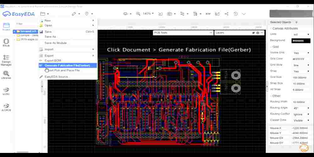
- Once the design is complete, export the Gerber files from the software. This can usually be done by selecting the “Gerber” or “Export” option in the software.
- Verify that the exported Gerber files are correct by using a Gerber viewer software. This step is crucial to catch any errors or mistakes that may have occurred during the export process.
- Zip the Gerber files and send them to the PCB manufacturer. Make sure to follow their specific guidelines for file naming and compression.
When creating a Gerber Design PCB, it is important to pay attention to the following details:
- PCB layer stackup: Make sure to export the correct layers for the PCB stackup, including copper layers, solder mask, and silkscreen layers.
- Drill files: Export drill files separately from the Gerber files, as they are used to create the holes on the PCB.
- Aperture files: Aperture files define the shapes and sizes of the copper features on the PCB. Make sure to export these files along with the Gerber files.
- Units: Gerber files can be exported in either metric or imperial units. Make sure to use the correct units for the PCB manufacturer.
By following these steps and paying attention to the details, you can create a high-quality Gerber Design PCB that meets your specifications.
Tools for Gerber Design PCB
When it comes to designing PCBs, having the right tools can make all the difference. Here are some of the top tools for Gerber design PCB:
1. Gerber Editors
Gerber editors are software programs that allow you to edit and view Gerber files. Some popular Gerber editors include GerbView, GC-Prevue, and ViewMate. These editors allow you to view and modify PCB designs, including layers, drill holes, and more.
2. PCB Design Software
PCB design software is essential for creating Gerber files. Some popular options include Eagle PCB Design Software, Altium Designer, and KiCAD. These software programs allow you to create schematics, layout PCBs, and generate Gerber files.
3. CAM Software
CAM (Computer-Aided Manufacturing) software is used to convert Gerber files into machine-readable formats, such as G-code. Some popular CAM software options include CAM350, GC-PrevuePlus, and BluePrint-PCB. These programs ensure that your Gerber files are correctly translated into machine instructions for manufacturing.
4. PCB Prototyping Equipment
Finally, you’ll need equipment to manufacture your PCBs. This can include a CNC machine, laser cutter, or 3D printer. Some popular options include the Bantam Tools Desktop PCB Milling Machine, the Full Spectrum Laser Cutter, and the Prusa i3 MK3S 3D Printer.
Overall, having the right tools is crucial for designing and manufacturing high-quality PCBs. With the right software and equipment, you can create accurate, reliable Gerber files that are ready for production.
Common Mistakes to Avoid in Gerber Design PCB
When designing a PCB using Gerber files, there are several common mistakes that can be made. Here are some of the most important ones to avoid:
1. Not Checking the Design Rules
Before generating Gerber files, it’s essential to check the design rules. These rules ensure that the PCB is manufacturable and meets the required specifications. Not adhering to these rules can lead to manufacturing issues and costly reworks.
2. Ignoring the Copper Thickness
The thickness of the copper layer on the PCB is vital in determining the performance and reliability of the board. Ignoring the copper thickness can result in issues such as poor signal integrity and high resistance.
3. Not Considering the Layer Stackup
The layer stackup is the arrangement of copper layers, insulation, and other materials in a PCB. Not considering the layer stackup can lead to issues such as crosstalk, impedance mismatches, and signal loss.
4. Overlooking the Drill Sizes
Drill sizes are critical in determining the size and placement of vias and through-holes. Overlooking the drill sizes can lead to issues such as misalignment, inadequate hole size, and drill breakage.
5. Neglecting the Solder Mask
The solder mask is a protective layer applied to the PCB surface to prevent solder from bridging between components. Neglecting the solder mask can lead to issues such as short circuits, component damage, and reduced reliability.
By avoiding these common mistakes, you can ensure that your Gerber design PCB is manufacturable, reliable, and meets the required specifications.
