Printed circuit boards contain a variety of electronic and electrical components. Some are analog, while others are digital and radio frequency. In addition to the components, printed circuit boards contain batteries, the basic element in any circuit. These provide the DC voltage needed for the circuit to operate. The type of battery helpful will depend on the circuit design and the application.
PCBs consist of copper or aluminum. However, both types of material have different properties. Aluminum-backed PCBs, for example, are often helpful in applications requiring high heat dissipation. In other cases, a standard substrate is coated with a heavy copper layer to increase the heat dissipation and circuit current capability.
Printed circuit boards were created for military applications but have since expanded into consumer electronics and industry. They are helpful in everything from medical devices to digital measuring equipment. They are also famous in automotive and aerospace applications. In addition to being useful in electronic devices, printed circuit boards can also help make other electrical and electronic components.
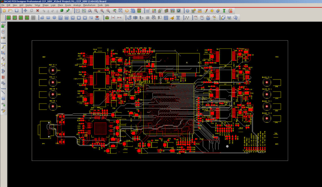
We construct printed circuit boards using multiple layers of copper, almost always arranged in pairs. The number of layers and the interconnection design determine the complexity of a board. More layers give more routing options and control over the integrity of signals but are more expensive to manufacture. The selection of vias also plays an essential role in determining the size and complexity of a board.
The Process of PCB Board Design
There are many different ways to create a PCB. There are multi-layer PCBs that sandwich internal layers. We also have four-layer PCBs, which offer even more routing options. Some layers are helpful as power planes and others as ground planes. The purpose of these layers is to increase signal integrity, decrease EMI, and improve power supply decoupling.
Schematic capture
Schematic capture is an essential step in the design process. It is the basis for electrical connectivity and is a legal document, meaning the design must be accurate, readable, and usable. During the schematic capture process, a schematic editor software interface helps to keep things organized.
During the schematic capture stage, electrical schematics are created, which depict how components and subassemblies are connected. These schematics are also helpful in conducting simulations using the software. These simulations can help identify potential problems and can also save a lot of time and money in the end.
Schematic capture is an integral part of the printed circuit board design process. It is a process that allows designers to convert a paper design into an electronic representation for use in circuit simulation and PCB design basics. During the schematic capture process, circuit components are organized into schematic sheets, and links are defined. A PCB design package can then help create a product design.
The schematic capture process also involves cleaning the bill of materials, which is a vital part of the PCB design process. It is essential in the volatile supply chain environment. In addition, it helps coordinate the mechanical and software design. The best PCB manufacturer know that a PCB layout must be manufacturable and Sourceable.
Schematic capture tools now integrate with third-party library services that offer online catalogs of thousands of parts. These services enable designers to download part data from these libraries easily.
How to Create a PCB layout Schematic Diagram
A PCB design Schematic diagram is a visual and logical representation of a circuit. It is the first step in the design process for an electronic product. In the past, designers would have to draw the circuit diagram by hand, but the availability of PCB design tools has simplified this process. The schematic should follow standard guidelines and include the components and their connections.
It is essential to label each symbol. These labels are transferred to the PCB layout and printed on the finished PCB. We should label the Schematic symbols with their name and value. To change the labels, click on them. If a schematic is too complex, a PCB assembly house may not be able to reproduce the electronic design. A schematic should cover several pages and have a clear flow. It should also include block diagrams.
When creating a PCB design Schematic diagram, remember to keep the original point as the center of a component. This will help you place components in the proper order. You should also name the file appropriately. You can do this by going to the properties of your components. Often, there are two different types of netlist files, and it is essential to use the right one.
Once you’ve finished with your PCB design basics, you can begin the process of having the PCB manufactured. Many PCB manufacturers will accept Gerber files or KiCad files. The Gerber file can be a good choice for PCB manufacturing, as it’s inexpensive and doesn’t require chemicals.
Schematic components
A PCB design Schematic should also contain a revision history. It should include a list of changes and comments made to the design. This section should be on the first or last page of the schematic. A table of contents is also essential, as it lists topics included in the schematic. However, this section may not be necessary if the design is simple.
A schematic diagram is a simplified version of a circuit board. It defines the electrical and logical connections between different components on the board. It also contains a netlist, which lists all connections in the design.
The design of a PCB should depend on a set of design rules. The design rules should establish the size of the printed circuit board, the spacing between lines, and power and ground lines. It should also specify the components that will be on the board. For example, the PCB should be small enough to fit inside the package and large enough to route the cable harnesses properly.
The PCB design Schematic is an essential document for any electronic product development. It should help you understand the components’ connections and your product’s overall functionality. In addition, a good PCB design will contribute to the quality of your finished product.
Layers
Layers in PCB layout design refer to the different layers of components on a board. The first two layers are copper foil and solder masks. The latter protects the copper foil by reducing conduction. The top layer is the silkscreen layer, which adds characters and Schematic symbols to the board.
The next two layers are the routing layer and the keep-out layer. These layers define the working area of the design and provide the designers with feedback. We may place them on the top and bottom layers of the PCB or internal layers. For more drill holes, four-layer PCBs are often a better choice. However, these boards are usually more expensive and have longer production times.
The base material of a PCB is called the substrate. The base material is insulating fiberglass, which provides strength to the PCB. Another layer on the PCB is the copper layer. The copper layer is helpful for the conducting path of various components. The copper layer thickness varies depending on the type of board. However, a good rule of thumb is copper sheeting at least eight layers thick.
The layers in printed circuit board design are critical to the success of a final product. The dimensions and dielectric material of each layer play a vital role in the functionality and performance of the final product. Depending on the design requirements, PCBs can have four, six, or as many as sixteen layers. The number of layers depends on the application, operating frequency, and pin density.
The physical dimensions of a PCB layout are known before the components are attached to the board. We attach them through a solder mask. Printed circuit boards may have a protective coating to minimize the possibility of shorts or corrosion of the copper layer.
Interconnections
There are various ways to improve the quality of interconnections in a printed circuit board design. The first method is soldering. This method has several advantages: simplicity, low cost, and reliability. The second method involves the use of connector clips. This method provides a more cost-effective alternative and is ideal for mass production and standardization. However, it has a few disadvantages, including the difficulty of replacement and maintenance. As a result, it is generally only applicable to components with fewer external leads. In addition, it requires more expensive components and may be unreliable. Nevertheless, it can reduce maintenance costs and improve utilization rates.
While implementing high-speed SPI communication, it is essential to consider the impedance of the signal layer. Insufficient termination can result in signal reflection at high speeds. In addition, an improperly terminated signal will flip phase 180 degrees. Therefore, it is essential to design high-speed interconnections using buffers and in-line resistors. This is because the amount of resistance on a PCB trace is directly proportional to its impedance. Therefore, a low-resistance buffer will consume a lot of currents, while a high-impedance layer will not influence the signal transfer.
Interconnections are essential to any electronic product. Even a printed circuit board can’t stand alone without other components. The best interconnections combine reliability, manufacturability, and cost. There are several kinds of interconnections, each with its advantages and disadvantages. Consider the following tips to choose the right one for your PCB design.
Increasingly dense electronic devices will need high-density interconnections. The printed circuit board design means more connections per unit area. In addition, it is possible to have more connections in a smaller space. However, HDI constructions are unavailable in all situations, and conventional constructions may reach their limits. This may require a new design strategy.
Placing components
Placing components correctly is a crucial aspect of printed circuit board design. Improper placement can cause circuit failures, shorts, and other problems. Furthermore, it can lead to delays in the manufacturing process. Proper placement can help minimize these issues and ensure that you correctly manufacture your PCB the first time.
When placing components on a printed circuit board, consider their location, function, and impedance. High-speed devices, for example, should not be placed close to the board’s edge. This is because the edges have different impedances and are more susceptible to electromagnetic interference. Additionally, high-speed traces should never cross over gaps in the signal return plane.
The placement of components on a printed circuit board is crucial for minimizing noise and other signal interference problems. In addition to keeping noisy signals away from sensitive components, logically grouping components can help prevent problems like solder mask and drill holes mishap. Furthermore, the placement of components in groups helps minimize traces’ length.
The next step in PCB design is to evaluate the schematic to understand how the circuit should function. Identify the different sub-sections and analyze each component’s voltage and current levels. This helps the designer to understand the flow of signals through the board.
Routing style
Routing style is an important consideration when designing a printed circuit board. A poorly routed board can result in short circuits and board cutoffs. Routing the board correctly is essential to prevent problems with overlapping signal traces. Using embedded analysis tools to check for power and signal integrity can help you change the board while routing. This prevents the need to redesign the board in the event of an error.
Impedance control is another important consideration when designing a PCB. It’s possible to get an accurate idea of what impedance is required by checking component datasheets and signaling standards. You can also use specialized applications to calculate impedance. For example, you can use differential pairs and single-ended pairs.
The printed circuit board size often determines the routing style in a printed circuit board design. Generally, a standard panel size of eighteen by twenty-four inches will be able to produce multiple PCBs. In the past, routing style helped make large PCBs. Later, other methods of PCB production were developed, including scoring, v-score, and routing.
Manhattan routing is another style of routing on a PCB. This method connects a trace on the X-axis to another on the Y-axis using a via. It also keeps all the horizontal copper traces on the same layer and all the vertical traces on a separate layer. This method has its advantages and disadvantages.
Achieving the right routing style on a printed circuit board requires careful consideration of details. Ideally, we configure power and ground paths to provide a clean signal return path.
How to Make a Printed Circuit Board

Many factors come into play when creating a PCB. These include component placement and routing, AOI, and component identifiers. Understanding these factors can help you make a better-printed circuit board. In addition, printed circuit boards are often the most expensive parts of a product, and a simple two-layer PCB will cost you about $100 to make.
Component placement
When designing a PCB, component placement is a critical issue. It affects PCB functionality and design, as well as its manufacturability and serviceability. Moreover, improper placement of components can result in poor analog signal quality. Therefore, following proper placement guidelines is critical to achieving the best results.
The proper placement of components can reduce the manufacturing process time and cost. However, incorrect placement may require extensive engineering time from the contract manufacturer or even the need to start over from scratch.
Component routing
Component routing on a printed circuit board is one of the essential design considerations for producing electronic components. Typically, a PCB contains many components arranged in a stepped array. However, board designers also avoid routing high-speed signal traces under large heatsinks.
The effect is a problem known as voltage-driven coupling. Voltage-driven coupling occurs when an active component is between a printed circuit board and a heatsink. The active component draws high-frequency current through a finite connection inductance. As the voltage of the active component is not equal to that of the board, the surface voltage of the component drives the board.
Component routing requires proper component placement. In addition, the spacing between parts must be adequate, we must optimize signal paths, and the board must pass manufacturability checks. Incorrect routing may result in errors that have ripple effects throughout the design.
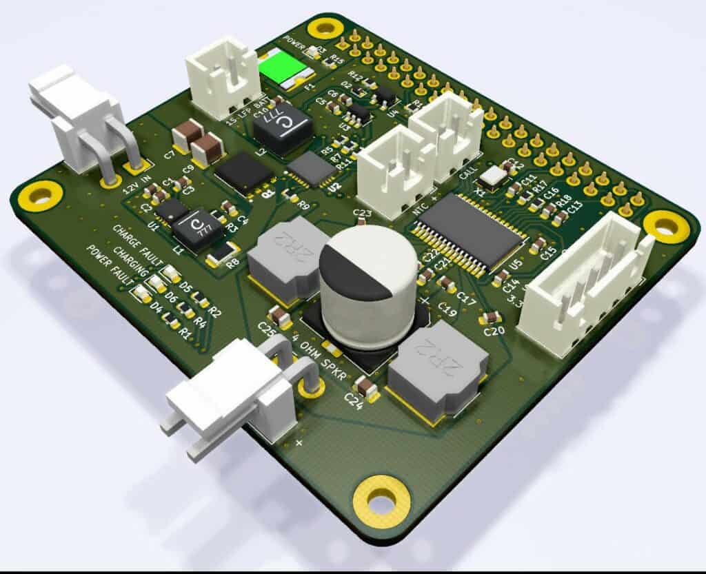
PCB Surface Mount Technology Assembly
Surface mount components assembly is placing electronic components on a PCB. The process begins with designing and picking components. The data for a printed circuit board then goes to the manufacturer. Different software tools are available to design a PCB, and they will then send it to a surface mount company to make it.
Component identifiers
When making a printed circuit board, it is essential to know which components belong where. Some components have a unique appearance and have a special identifier. For example, transistors have a “D” shape and a marking indicating which way the current flows through them.
The ID of a PCB component is usually found on the datasheet, a document that identifies the components inside. This document includes the component’s identification and manufacturer part numbers (MPN). The manufacturer’s part number is the same as the part’s, facilitating easy reference to the correct part. The data sheet will also contain a drawing of the PCB’s land pattern, which helps create the board’s footprint.
AOI
Automated optical inspection is a critical step in PCB assembly. After assembling the PCB, errors are not easy to repair. The automated optical inspection machine compares the printed circuit board to a model provided by the manufacturer. Once it passes inspection, the PCB moves on to the final steps of PCB manufacture.
Automated optical inspection can speed up the inspection process. AOI can identify potential PCB errors by checking for surface defects, component placement, and dimensional accuracy. Manual inspection becomes impossible as printed circuit boards become increasingly complex and intricate. AOI can help manufacturers improve the quality of their products at a low cost.
Design rule check
Design rules check-in PCB layout are vital in converting a two-dimensional schematic into a physical product. They help ensure that components are in the correct place and that their layout fits the manufacturing parameters. There are several ways to perform design rule checks in PCB layout.
First, a design rule check identifies any design limitations. This step helps designers set parameters for trace width, component spacing, and via diameters. Afterward, they can complete the design process. The design rule check also flags manufacturing-specific constraints.
Etching
Etching a printed circuit board is an excellent way to make the components in your electronic devices look better than they ever have. The process is relatively easy and involves a couple of different steps. First, you need a solution that contains 3% hydrogen peroxide. The solution should cool down before being helpful. Next, stir it with a wooden stick to speed up the etching process. You can also stir it with metal objects but do so cautiously. After this process, you can discard the solution or use it again.
To make an etched board, you will first need a conductive liquid. Next, you can buy a liquid etching solution or use a powder. Once you’ve found a solution that will work for your board, prepare the board for the etching process. Most PCB etching solutions require a few hours of soaking, and you’ll need to stir it for a few minutes after each step. The solution should be about 50 to 70 degrees Celsius and contain enough chemistry to cause an etching effect. If you don’t have this type of solution, you can always use matches to heat it.
PCB Design Optimization
PCB design optimization can save time and money by reducing the number of layers and reducing the number of wire-to-board connectors. In addition to reducing the number of layers, wire-to-board connectors should be at the edges of the PCB, where they reduce the chance of damaging the surrounding components. PCBs are getting smaller, which means space is a precious commodity. In addition, placing all the components on one layer minimizes the time it takes to install them and reduces the assembly cost.
Xpedition Path Finder suite
The Xpedition Path Finder suite provides an industry-leading new path-finding methodology for PCB design optimization. It offers comprehensive, automatic planning of chip connectivity through multiple packaging variables and targets multiple PCB platforms. The software also provides a single, integrated circuits design optimization environment.
Xpedition Sourcengine
Xpedition Sourcengine PCB Design Optimization combines powerful design optimization and automation capabilities to help engineers develop complex electronics and systems. Its comprehensive solution supports multi-enterprise environments, enables collaborative design across different disciplines, and reduces design spins and rework. It also supports the design and verification of complex multi-board systems.
Advanced Performance Metrics
PCB Thermal Solver is a powerful tool that allows designers to simulate voltage and temperature distribution along copper traces. The software also identifies potential hot spots on power stage components. These simulations help identify the remaining design problems before final signoff. By comparing simulation results to real-world measurements, designers can determine the best thermal solution for their PCB.
Thermal design requires the use of a large number of PCB layout patterns. In that case, a method such as Bayesian optimization is useful. It is faster than traditional algorithms and can find the optimal layout for a given problem from up to 10 million layout patterns.
PCB pad design elements
To optimize the PCB design, it is essential to use the right PCB pad sizes and shapes. When making a PCB, many factors determine the size of the pads, including the components’ shape and size, the type of substrate, and the manufacturing process helpful. For this reason, PCB pad design is critical to the reliability of the SMT product. Fortunately, there are several design standards for PCB pads, including the IPC-SM-782A standard. Nevertheless, developing your design specifications is still recommended if possible.
Shielding
Shielding is essential to any electronic device, as it protects the circuits from unwanted signals and EMI/RFI emissions. In today’s technologically dependent environment, shielding is necessary for every item. Harwin offers EMI/RFI shielding services and solutions for your PCB designs.
We achieve the shielding of a PCB by placing copper layers on the board outline. These layers connect through stitched vias. The signal layers are between these two layers. A solid copper layer provides better shielding, while cross-hatched copper traces provides flexibility without sacrificing signal integrity.
Working current
Having an understanding of the working current of your PCB is crucial when designing an electronic circuit. Often, the current flow on the board is difficult to predict, which leads to electrical noise and other issues. For this reason, you should avoid putting significant energy components near the board’s edge. These parts can accumulate heat and increase board temperature. Instead, position your microcontroller near the center of the board outline, where the heat can disperse.
Using Ohm’s law, you can determine the working current of a printed circuit board by dividing the voltage by its resistance. Early printed circuit boards have point-to-point jumper wiring. Today, however, the spread copper layer is helpful to optimize space and isolation from low-power rails.
Layers
There are several different kinds of layers on a PCB. They are helpful for various purposes, including thermal conductivity and reliability. They also help reduce inductive and resistive losses. However, each manufacturing process has different limitations and constraints. Therefore, it is essential to determine the right amount of space between layers and ensure that all components are within a specific distance from the edge of the board.
The first step is to determine the number of layers. The number of layers depends on the power level and complexity of the design. More layers may be necessary if the PCB needs a lot of power. For example, short digital clock traces should not cross over a signal return plane gap if a high-speed digital clock is present.
