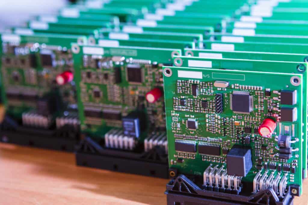
Printed circuit boards are the core of electronics. They are the framework upon which electronic devices are built. Therefore, they play a crucial role in electronic manufacturing. Also, PCBs offer mechanical support and electrical connection to electronic components. You will find PCBs in devices like computers, smartphones, industrial equipment, and more.
When you detach an electronic device, you will notice a green board. The green board in this device is a printed circuit board. It is crucial to understand how these boards function in electronic devices. Therefore, this article seeks to explore every detail about PCB electronics.
What is PCB Electronics?
A printed circuit board is an electronic board that offers electrical connections to components in a controlled manner. These boards are also known as printed wiring boards. Components such as capacitors, semiconductors, and diodes are mounted on the board. Furthermore, PCBs feature electrical and mechanical characteristics that make them suitable in several applications.
PCB electronics is an emerging PCB technology that helps to reduce electronic packaging expense. Also, circuit boards were earlier developed in the 20th century. However, this board has experienced rapid development over the years. Before the advent of PCB electronics, traditional wired circuits were commonly used in electronic devices.
Printed circuit boards can different layers. The single layer board is ideal for use in simple electronic devices. However, circuit boards used in complex devices like motherboards can have several layers. Circuit boards are usually green in color, however, they can have another color.
PCB electronics usually comprise layers. These layers include substrate, copper, silkscreen, and solder mask. Therefore, a PCB is similar to a lasagna or layer cake in which there are alternating layers of various materials. Also, the engineer etches the layers separately and laminates them together to create patterns called traces. The PCB passes through a lamination process whereby the layers are laminated with adhesive and heat.
A schematic diagram displays the PCB layout in the design stage. PCBs are available in many sizes and shapes based on the requirements of their applications.
Layers that Make up PCB Electronics
Substrate layer
The substrate layer is often made from fiberglass. It is responsible for the rigid form of the circuit. Also, most boards feature this material as their substrate. FR4 is known as the most frequently used material for a PCB substrate. Their rigidity and thickness help to form the PCB. Also, the substrate layer can comprise other materials kike epoxies. However, epoxies are not as durable as FR4.
Copper layer
This is a layer of copper foil. Also, the PCB manufacturer uses heat to laminate the copper foil to the board. When we talk about different types of layered PCBs, we refer to the number of copper layers in a board. For instance, a single sided PCB comprises a layer of conductive material. This material is on one side of the board.
However, double sided PCBs have two layers of conductive materials. Each of these layers are mounted on each sides of the board. Also, double sided PCBs enable closer routing traces. The power requirement of the PCB will determine the copper thickness.
Soldermask layer
The PCB manufacturer places this layer on copper layer. Soldermask is responsible for the green color of printed circuit boards. Also, the soldermask layer insulates the copper, thereby preventing it from having contact with other elements or metal. It helps manufacturers to solder the right areas on the circuit board. Solder mask is usually green in color, however, there are other colors like red.
Silkscreen
The silkscreen layer is usually applied on the soldermask layer. Also, this layer helps us to understand the functionality of several LEDs or pins on the board. Silkscreen includes symbols, letters, as well as numbers to the printed circuit board. Also, silkscreen usually comes in white color. However, there are other colors like gray, yellow, and black.
Types of PCB Electronics
There are different types of printed circuit boards in terms of the number of copper layers and flexibility.
Single layer PCB
This type of circuit board has one conductive layer. This means that there is only one conductive copper layer on the substrate. Also, single layer printed circuit boards are commonly used in simple devices like FM radios, calculators, and LED lighting boards.. These boards have electrical components soldered on one side. The conductive paths can’t overlap since these PCBs feature one conductive layer.
Double layer PCB
This type of PCB features a thin layer of copper on both bottom and top sides. Plated holes in the substrate provide connection to the two sides. Also, double layer PCBs are ideal for use in various applications like test equipment, UPS system, and cell phone systems among others.
Multilayer PCB
Any circuit board that has more than two copper layers is a multilayer PCB. This board has at least three layers of copper. All of these layers are carefully laminated under extreme temperatures and pressures. Also, multilayer boards offer a high level of design flexibility. These boards are ideal for high-speed circuits.
Flex PCB
A flex printed circuit board comprises several components and circuits placed on a flexible substrate. Also, flexible circuits are usually made from polyester film or polyamide. These circuits are specially designed to bend, fold, or twist in a desired form. Flexible boards are available in different types of layers.
Rigid PCB
This is a circuit board that features a rigid substrate as its base material. Also, the rigid substrate gives the board a required level of strength and rigidity. Also, rigid PCBs comprises several layers which are carefully laminated with heat and adhesive. Rigid boards are ideal for use in X-ray machine, laptops, and more.
Rigid flex PCB
A rigid flex printed circuit board combines the features of rigid and flexible circuits. Therefore, you can bend or twist this board. Also, you can shape this board or curve it during manufacturing. The flexible part of this PCB enables interconnections between the rigid boards. Therefore, it gives room for marrow conductor lines that takes less space. You can design rigid flex PCBs in a lightweight and compact manner.
High density interconnect (HDI) PCB
HDI PCB is a type of PCB electronics that features higher wiring density for each unit area. It is different from conventional PCBs. This board has finer lines and spaces and higher connection pad density. HDI PCBs are ideal for improving electrical performance as well as reducing size and weight of devices. Also, these boards have high density features like high performance thin materials and laser micro vias.
Common PCB Electronic Problems
There are some problems commonly associated with PCB electronics.
Plating voids
Plating voids results from the deposition on a board. Also, any fault in sedimentary impact the hole walls’ integrity. Therefore, this prevents the circuit board from functioning as expected. Also, plating voids can occur as a result of uneven copper coating. This may happen due to contamination, rough drilling, and air bubbles.
Furthermore, there are ways to avoid plating void. The best way is to perform a smooth drilling process. Follow the directions provided by the manufacturers to achieve this. Also, this includes the drill speed and the number of drill hits.
Inadequate copper to edge clearance
Copper is a raw material used in PCB manufacturing. Also, copper is a highly conductive material. However, it is prone to corrosion. The best way to prevent corrosion is to isolate the copper. However, inadequate copper to edge clearance occurs when copper is very close to the edge. Therefore, this exposes the copper and result in the malfunctioning of the printed circuit board.
You can prevent this problem by ensuring there is adequate space between the copper and the PCB edge. There won’t be any risk of trimming the copper along with the circuit board. Also, you can use DFM software to set some clearance standards.
Lack of DFM
DFM simply means design for manufacturability. It is a crucial part of PCB manufacturing. Also, DFM software is capable of solving any design problem before beginning the manufacturing process. Furthermore, DFM makes it much easier to detect problems in the PCB structure. It will be difficult to figure out issues in printed circuit boards without the DFM software. Therefore, it is crucial to invest in DFM analysis tools to prevent these problems.
Design Problems Encountered in PCB Electronics
Silver in PCB
Copper has the ability to corrode due to its soft texture. It is crucial to avoid silver in printed circuit boards in order to preserve their structural integrity and as well prevent corrosion. Gold is an ideal material for PCB electronics. This material is malleable and is ideal for use in a variety of electronic components.
Acid traps
Etching is a crucial step in PCB manufacturing process. It involves the removal of extra copper from printed wiring boards. There are different types of acidic materials you can use to remove copper. However, etching can result in acid traps formation. This is a big problem as the acid can cause corrosion in the copper tracing and other PCB components.
Ensure traces are well placed during etching. Also, it is crucial to maintain an ample distance between vias and the paths.
Missing solder masks between pads
Sometimes, there can be missing solder masks between pads. This can result in solder bridges formation. Therefore, it is advisable not to allow solder masks between pins or pads.
Electromagnetic issues
These issues can occur due to irregularities in electromagnetic interference (EMI). PCB manufacturers must fabricate PCBs that reduce the impact of EMI. Therefore, it is advisable to increase the PCB’s ground area to minimize cross-talk, noise, and emission rate. Also, you can separate the analog and digital component of the PCB to categorize EMI.
Insufficient annular rings
The creation of vias involves drilling through pads on each side of the PCB and then plating these holes to create connection between the two sides of the PCB. The via may not function as expected if the drill hole takes a large space on the pads.
PCB Fabrication Process
The PCB fabrication process involves the creation of bare boards in which electronic components will be carefully assembled. Also, It is important to note that PCB fabrication is entirely different from PCB assembly. Both PCB fabrication and PCB assembly are aspects of PCB manufacturing process. PCB fabrication simply involves transforming a PCB design into a physical board. The PCB design is the first stage of PCB manufacturing.
On the other hand, PCB assembly involves placing components on a bare board. The components placed on this board are responsible for its functioning in electronic devices. Therefore, we consider PCB fabrication as a path to building a city. Also, PCB assembly is the actual board that makes a PCB operate. Before commencing with the PCB fabrication process, you need to complete the PCB design. Below are the steps in PCB fabrication:
Laser direct imaging
Laser direct imaging is usually applied in areas of the PCB that will become traces. Here , the PCB fabricator applies a dry film to the copper laminate. Then the LDI exposes some parts of the PCB to light. The unexposed parts of the PCB will create an etch barrier. Also, this barrier will be carefully removed to create copper circuitry.
Oxidation and lamination
After etching all the layers, the fabricator applies a chemical treatment known as oxide to the inner layers of a PCB. This helps to enhance the bond strength. After this, the layers of copper foil and prepreg pass through the lamination process. This process involves the use of a hydraulic press and heat.
Drilling
The next step is drilling of holes in the circuit board. Also, the holes help to create vias which serve as a connection. The type of via used will determine the size of drilling. However, drilling is usually carried out on a stack of 2 to 3 panels. Furthermore, the fabricator plates these holes with copper. This helps to transfer electrical signals.
Electroless copper deposition
This step involves using mechanical and chemical processes to get rid of excess debris and resin. After removing the debris and resin, the fabricator deposits a thin coat of copper on the exposed areas of the panel. Therefore, this forms a metallic base that helps the electroplating process.
Plating, stripping and etching
Electroplating involves dipping the panel in a copper plating bath. This bath is a mixture of copper sulfate and sulfuric acid. The copper deposits on the PCB’s surface. After this, the fabricator removes the plate and dips it in a tin plating bath. This acts as an etch barrier.
After plating, you will need to remove the dry film and etch the exposed copper. The pads and traces on the plate are usually left untouched.
Soldermask application
The PCB fabricator applies solder mask on the board. Also, soldermask protects the copper, thereby preventing it from having contact with other elements or metal. The soldermask gives the PCB the green color. It is a layer of polymer that prevents the copper traces on the PCB from oxidizing. Also, soldermask helps to prevent solder bridges from occurring.
Soldermask is available in different colors. However, the most commonly used color is green. This color has trace visibility and high contrast. The color of soldermask doesn’t affect a board’s functionality. However, darker colors are a better choice as they are heat-absorbent.
Silkscreen application
After applying the solder mask, the PCB fabricator applies silkscreen on the PCB. Silkscreen adds board markings and component reference designators. Also, silkscreen helps to identify some pins on the board. After this, the fabricator bakes the PCB in an oven in order to cure the silkscreen ink and solder mask.
Surface finish
Surface finishes are important in PCBs as they help to protect metal. The fabricator applies surface finish to any exposed metal surfaces. Also, there are different types of surface finishes like immersion gold, tin coating, silver coating, and more.
PCB Assembly Process
The PCB assembly process involves the mounting of electrical components on the bare PCB board. Also, PCB assembly is an aspect of the PCB manufacturing process. There are two different mounting technologies usually integrated in PCB assembly. These are surface mount technology and through hole technology. Also, the end result of the PCB assembly process is an assembled circuit board.
Surface mount technology (SMT)
Surface mount technology (SMT) uses an automated process to install electronic components on a circuit board surface. Also, SMT uses a pick and place machine to directly place surface mount device on a bare circuit board. This technology has a lot of benefits. Surface mount technology is a faster process that enables the production of complex electronic devices.
Through hole technology (THT)
THT involves drilling holes on a PCB. Also, the THT process involves mounting through hole components with leads by integrating plated through holes. The PCB assembler inserts pin through holes in circuit boards. Also, THT offers great advantages. For instance, a through hole offers stronger connections.
Steps involved in PCB Electronics Assembly Process
Solder paste application
This step deals with the application of solder paste on the bare circuit board. Here, the PCB assembler places a stencil over the circuit board. This helps to ensure solder paste is evenly applied to where components will be placed.
Pick and place
You can perform component placement can manually or automatically. In THT, the assembler places the components manually. However, surface mount involves the use of automated pick and place machine. This machine makes component placement precise, error-free, and quick.
Soldering
SMT involves reflow soldering. Here, the PCB moves through a reflow oven while the solder paste melts. The temperature in the oven is responsible for the liquefying the solder paste. After then, the molten solder passes through a cooler where the solder becomes solid.
On the other hand, THT integrates wave soldering. Here, the PCB passes over a wave solder liquid. Wave soldering liquefies the solder and then solidifies it in a cool temperature.
Inspection
Inspection is very necessary in PCB assembly. It helps to evaluate the functionality of the board. There are several inspection methods integrated in PCB assembly. These include X-ray inspection, visual inspection, and automatic optical inspection.
Use Cases of PCB Electronics

PCB electronics are appropriate for use in several applications. The properties and benefits of PCBs are the reasons they are widely used across several industries. You will find PCBs in most modern devices.
The commonly used PCBs in the aerospace industry are rigid flex, flex, and rigid boards. Also, these boards are widely integrated in flight controls, safety systems, and instrument panels among others. The advancement in the aerospace industry has helped to increase the demand for more complex circuit boards. Flex and rigid circuits provide the level of flexibility, mission survivability, and durability needed by aerospace devices.
Industrial equipment
PCB electronics have been able to revolutionize the supply chain management system, thereby increasing automation and efficiency. This system is a reliable way of directing equipment in automated facilities.
Medical
PCB electronics have contributed to the advancement in medical electronics. Medical devices like radiation equipment, imaging systems, and MRI machines feature printed circuit boards. Also, flexible and rigid PCBs enable the manufacturing of lightweight and compact devices like implantable devices and hearing aids.
Military
The military sector also benefits from PCB electronics. Military devices are often exposed to vibration and impact. Therefore, military PCBs are specifically designed to withstand a high level of shock and vibration. Military devices like modern weapons, military vehicles, and rugged computers feature high performance PCBs.
Consumer electronics
A wide array of consumer electronics feature printed circuit boards. These boards are responsible for the functioning of consumer electronics. Most simple consumer electronic feature single sided PCBs. PCBs are available in devices like smart phones, televisions, and radios among others.
Conclusion
We have provided vast details about PCB electronics and their function in electronic devices. A professional PCB company can cater for all PCB fabrication and assembly needs. As PCB solutions provider can meet all your requirements and specifications for your PCB electronics. Order PCB electronics from us today and get the best quality PCBs.
