There are many printed circuit boards, and they all serve different purposes. Some are rigid, while others are flexible. The most common type of PCB is the fiberglass-cored rigid board. Rigid boards are easier to manufacture and can fit into tight spaces, while flexible ones can’t bend as much and can’t be helpful for sensitive applications.
PCBs usually have a copper layer, and one layer is the solder mask. Another layer is the silkscreen layer. This layer is typically white and adds information to the PCB. This information can include symbols, function notations, and other information. This layer makes the PCB easier to assemble and use.
PCBs are a fundamental element of all electronic devices. They make it possible to downsize electronic devices while allowing for incredibly powerful circuitry. Today, printed circuit boards are in virtually every product you own, including smartphones, computers, vehicles, music players, smartwatches, and industrial machinery.
The basic circuits in a bare board can vary significantly in function and size. Therefore, the size and shape of the board are often crucial to the device’s functionality. Printed circuit boards have different materials and are multi-layered, single-sided, or double-sided. Each type of printed circuit board PCB has different benefits and functions.
Electronic components assembly Process
If you have a knack for electronics, you can learn how to make circuits by connecting components. A breadboard is a simple plastic board with short metal lines that can help create circuits without soldering. Instead, wires connect different components and can come in different colors and lengths. Some have clips or clamps on one end to connect them to other components.
Wires
A circuit is a series of connected parts. In a circuit diagram, a symbol represents each part. The connection between two components uses a line. A line represents a perfect conductor because it carries no resistance. A line also touches all the components or source terminals at the same voltage. A circuit diagram usually includes dots to indicate connections between the lines. For example, the wire is curved around the resistor when a component is connected to another. On the other hand, a switch breaks the circuit and closes the current path.
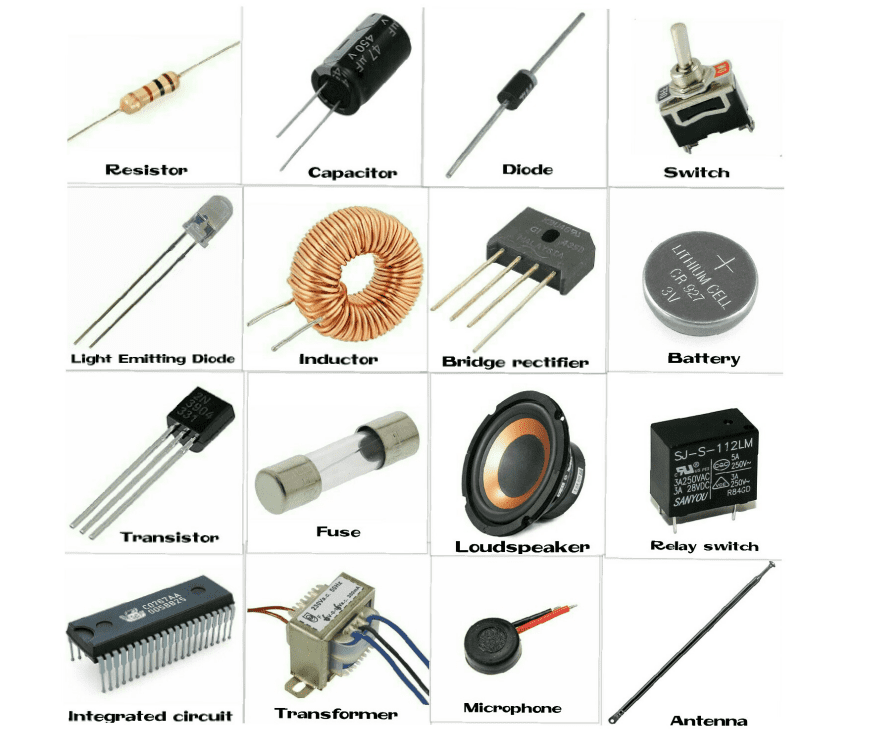
Diodes
When forming an electronic circuit, one of the most fundamental elements is the diode. This electronic component comprises two semiconductors – p-type silicon and n-type silicon – and connects in series. Next, a resistor is placed between the two semiconductors, limiting the current flow between them.
Diodes help convert AC power into DC. For example, a full-wave rectifier uses four diodes to do this. The diodes pass half of the AC waveform, which then charges a capacitor. The capacitor then produces a steady DC current. This process is called voltage amplification, and different combinations of diodes and capacitors can help create different types of voltage multipliers.
Transistors
Putting together a circuit involves connecting electronic components. There are two basic ways to connect components in a circuit: series and parallel. In series connections, the components are connected end to end, allowing the current to flow through them sequentially. A simple example of a series connection is a string of lamps.
Circuit diagrams depict the connections between the components, and the symbols used to represent each component has their names. For example, ‘C1’ would refer to the first capacitor, while ‘L1’ would refer to the first inductor, Q1 to the first transistor, and so on. The component’s value would be alongside it, and detailed specifications would be on the parts list. International standard IEC 61346 gives detailed rules for how to label circuit components.
Capacitors
A capacitor is a device that stores energy. It is not as large as a battery but has a much longer life and can deliver energy faster than a battery. For example, the flash of a digital camera uses a capacitor. Capacitors are also helpful in power supplies, transceivers, and amplifiers.
One way to connect capacitors in a circuit is to connect them in a series. Using a series connection, each capacitor stores the same amount of charge. Because each capacitor has the same charge, the current going through them will be the same. When we apply voltage to a series of capacitors, electrons shift from one plate to another.
Using series and parallel connections, capacitors connect in a network. Therefore, increasing the number of capacitors in a parallel circuit will increase the total capacitance of the circuit. Capacitors in parallel are connected similarly to resistors in a series circuit.
Inductors
Inductors are electrical components that generate an opposing magnetic field when current flows through them. The current changes the strength of this magnetic field, and the magnetic flux changes direction in response. They help resist this sudden change in current flow. Inductors have the letters L and H.
Inductors integrate into integrated circuits (IC). ICs are devices with resistors, capacitors, diodes, and sensors. Inductors consist of coils and wires wound around a core. They can also be air or metal and consist of spiral wires. They are typically smaller in size than ICs but have the advantage of low loss and noise compared to coils and spiral inductors.
When the current flows through an inductor, it creates an opposing force called the back EMF. As a result, the current flows through the inductor from the battery. As more current flows through the inductor, the magnetic field fades.
Types of Printed Circuit Boards
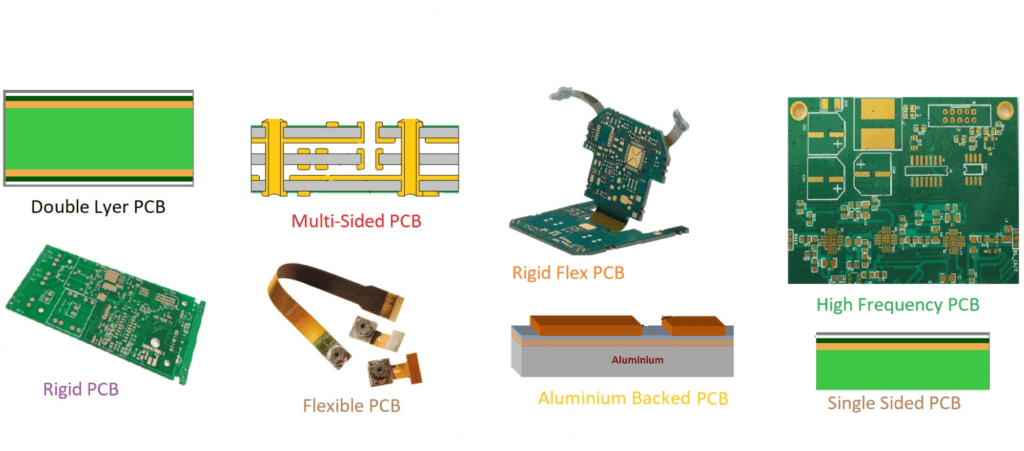
There are three types of printed circuit boards. The flexible and rigid types are helpful for various electronic applications. These are helpful in small-sized and low-electricity items. They are often less expensive than other types but are limited to items that are not highly sensitive to electricity.
They are typically helpful in computers, mobile phones, GPS equipment, and personal entertainment devices. In medical applications, they are often beneficial in MRI and CAT scans. Other applications include temperature sensors and control tower instrumentation.
Single-Layer PCB
Single-sided printed circuit boards, or PCBs, are helpful in electronic equipment. They offer mechanical support for electronic components, electrical connections, and insulating material. The materials used in PCBs vary in thickness and are usually copper. The material is strong, making them resistant to breakage and bending. PCBs can also include identification characters and automatic solder mask.
Single-sided PCBs are simple to produce and are often essential in low-cost electronic products. However, if you are making a more complex electronic product, you may want to consider double-sided boards. The latter is often more powerful and can withstand higher heat and power levels.
Single-sided PCBs can also consist of a high-grade finish. A higher-grade finish is more durable and can make the board low-cost. Additionally, the board’s size and the number of through-hole components will affect the final cost. Tinniness is also an issue and will increase the price of the board.
Single-sided PCB design has copper traces that serve as the basic structure of circuitry. In addition, these signal traces have a coat of various materials that help protect the copper from oxidation and corrosion.
Multi-layered
Multi-layered printed wiring boards are helpful to accommodate more electronics. They range from four to twelve layers. Smart devices typically use four to eight alternating layers, but higher-end mobile devices often use twelve or more layers. The right number of layers is critical for achieving high-performance electrical signals. Incorrect PCB design and material selection can reduce performance and cause crosstalk or emissions.
Multi-layered PCBs are helpful in many military, medical, and industrial systems. Their lightweight and high-performance capabilities make them a popular choice for these applications. Multilayer PCBs are also used in aerospace and automotive systems, as they can handle harsh environments and maintain quality and functionality.
Unlike single-layer boards, multi-layered PCBs have two reference planes and one signal plane. This stitching via reduces the area available for the signal to travel between alternating layers. Different types of vias can be helpful, such as buried, blind, and standard. They can withstand high-temperature conditions and are well-connected and are good insulating material.
Rigid-flex
Rigid-flex printed circuit boards (PCBs) have a flexible, bendable structure and multiple layers. In addition, we can partially route flex boards with break-away tabs that allow the circuits to remain in the panel during component assembly and wave soldering processes.
Another benefit of rigid-flex circuit boards is their small size. They are ideal for applications requiring minimal space. The smaller overall size of these boards can eliminate the need for additional connectors and cables. Additionally, they are less expensive to produce and assemble, making them ideal for smaller devices.
Rigid-flex PCBs are often helpful in military and aerospace printed circuit board fabrication. This is because they are flexible enough to fold and bend without damaging components. Because of these features, rigid-flex PCBs can be helpful in applications that require ultra-thin packaging. For example, rigid-flex PCBs are essential in high-end aircraft-mounted weapon guidance systems.
Rigid-flex PCBs are a hybrid of rigid and flexible board technology. They consist of several layers of flexible circuit substrates attached to a rigid board. In addition to being able to bend, they are durable enough to withstand the abuse of the field.
How to Design and Make a Printed Circuit Board assembly

The first step in the PCB assembly process is to create a design database. This database allows you to store and organize the schematic and net connectivity information. Once you have the schematic, you can place component footprints in your CAD system.
Surface mount is a type of PCB design in which the components are placed on the surface of the board. A surface mount device address the growing demand for smaller components and faster PCB manufacturing. Instead of mounting the components through holes, wire leads are placed on the surface of the board. This eliminates the need for holes in the board and gives the circuit board more space for mounting components.
Dimensions of a printed circuit board
Several factors should be taken into account when designing a printed circuit board. One of the most important is the copper weight of the board. Copper weight is the thickness of the copper tracks on the board. Generally, manufacturers offer a choice of 0.5 oz (17.5 um), 1.0 oz (35 um), or 2.0 oz (70 um) copper thickness. Naturally, the more copper there is on the board, the lower the track resistance.
Different printed circuit boards have different sizes, so it is essential to know how much board you need. A thick board is more durable, while a thin board is more flexible. Thin boards are brittle and can break easily. A thicker board is better suited for a computer motherboard.
Identifying components on a printed circuit board
The first step in identifying components on a PCB design is to identify the board itself. Some boards have codes or references that will help you identify what the board is for. For example, a DMCB board is the DOS Main Control Board on a GE Mark V computer. In addition, many other acronyms can help you understand what the board is helpful for. Other PCBs are daughterboards, small boards that attach to a motherboard and give access to the CPU or memory.
Identifying components on a printed circuit board design is essential to electronic engineering. A PCB design is composed of many different layers, each with its function. When creating a printed circuit board design, the manufacturer must choose the most appropriate material for the PCB design. For example, some PCBs use paper bases or glass-fiber cloth as the base.
Transistors are one type of semiconductor that is helpful in electronics. They help in switching electrical power and amplifying signals. They have three terminals and a “D” shape. Transistors are a key component of electronic circuits because they control current flow.
Creating a schematic for a printed circuit board
Creating a schematic for a printed board is a fairly simple process. The first step is to convert a PCB into a schematic diagram. You can do this by utilizing a CAD tool that can create a BOM. Next, you can input data such as the vendor part number and name to create a complete BOM. There are also several steps to follow when creating a schematic, including using a checklist.
One of the essential steps in creating a schematic is identifying the components. Then you can move them to logical positions in the schematic. You may need to replace lines or pull out components to create a more logical layout.One can also remove unnecessary points to make corners sharper. You can also use a multimeter to check the connections in the inner layers to verify if everything is still logically connected.
A schematic is essential for creating a PCB layout and should be created before you begin designing the PCB footprints. If you don’t have a PCB schematic, you may encounter issues with electrical conductivity. It also serves as a visual representation of the board and can be a helpful reference for the layout.
Types of Printed Circuit Board Materials
Printed circuit boards consist of a variety of different materials. The base of these boards is typically composed of a laminate or substrate. The substrate is a non-conductive material and serves as a core material. The electronics are then positioned on this board and soldered to the circuits. In addition, contact fingers are often included on the edges of these boards to serve as connectors for other PCBs or external devices.
The materials used for PCBs differ in their electrical and mechanical properties. For example, some types of laminates and reinforce are made of glass, paper, and fabrics, while others consist of thermosetting plastic resins. The thermosetting resins are typically used for microwave applications, while the phenolic types are generally less expensive and suitable for many other applications.
The most common type of PCB material is FR-4, a fiberglass-epoxy laminate. Its high tensile strength and low dielectric constant make it a popular choice for PCBs. FR-4 laminates are also flame-resistant and do not absorb moisture. As a result, they retain their thermal performance even in humid and dry environments.
Polyimide is an excellent flexible circuit substrate available in white, black, and transparent colors. It is relatively inexpensive and has a low thermal expansion coefficient. It is also highly elastic, making it a popular choice for flexible boards. Advanced polyimide and polytetrafluoroethylene are also available.
The Difference Between Rigid-Flex PCB and Flexible PCB

A PCB is an essential component of any product or device. It can be rigid or flexible. The choice depends on the application. Rigid-flex PCBs are more durable but require more material. These boards have rigid layers to withstand high temperatures and are not as bendable as flexible boards.
The substrate material for rigid PCB is also critical to its performance. Flexible circuit sheets consist of flexible dielectric and glue films.
Flex circuit boards are generally more expensive than rigid circuit boards, but they allow engineers to make more compact products. In addition, flexible PCBs can be bent or folded to fit tight spaces, which is especially beneficial for portable products. However, flexible circuits are less durable than rigid PCBs and unsuitable for high-density circuits.
When it comes to weight, rigid PCBs are heavier and more fragile. As a result, they are not as durable as flexible PCBs, but their superior resistance to high temperatures and extreme environments make them the perfect choice for small devices.
Rigid PCBs have a rigid base, while flexible PCBs can bend or twist. Flexible circuit boards are flexible and can be helpful in any configuration. They also require less space than rigid PCBs. They are often beneficial in mobile devices, networks, and 5G/6G communication equipment. Flexible PCB is also helpful in many computer components.
Rigid-flex structure
Rigid-flex PCBs have a flexible, bendable structure and multiple layers. In addition, we can partially route flex boards with break-away tabs that allow the circuits to remain in the panel during component placement and wave soldering processes.
Another benefit of rigid-flex circuit boards is their small size. They are ideal for applications requiring minimal space. The smaller overall size of these boards can eliminate the need for additional connectors and cables. Additionally, they are less expensive to produce and assemble, making them ideal for smaller devices.
Rigid-flex are often helpful in military and aerospace electronics manufacturing processes. This is because they are flexible enough to fold and bend without damaging components. Because of these features, rigid PCB industry can be helpful in applications that require ultra-thin packaging. For example, rigid-flex are essential in high-end aircraft-mounted weapon guidance systems.
Rigid-flex PCBs are a hybrid of rigid and flexible board technology. They consist of several layers of flexible circuit substrates attached to a rigid board. In addition to being able to bend, they are durable enough to withstand the abuse of the field.
Application of PCB Circuit Board
A PCB circuit board is a printed circuit board that helps build electronic devices. The printed circuit board consists of layers that are permanently connected. The PCB is usually green in color. However, it is also available in other colors. Several processes help apply the printed circuit board.
PCBs can consist of different layers, including inner copper layers. In addition, some internal layers are helpful as power and ground planes. This allows for better signal integrity, lower EMI, and improved power supply decoupling.
We determine the thickness of a PCB by the amount of copper foil on it. The weight of copper per square foot is a good guide for determining the thickness of a PCB. One ounce of copper per square foot equals 1.344 mils or 34 micrometers. A layer that exceeds three ounces of copper per square foot is considered heavy copper foil. A heavy copper layer can provide high current carrying capacity and heat dissipation.
PCBs are helpful in many different types of equipment. Some examples include measuring equipment that monitors pressure and temperature, electrical scales, and speedometers. Other applications for multi layer PCBs include audio and video devices, such as FM radios and USB systems. Automotive electronics also use multi-layer PCBs extensively. For example, today’s vehicles include several electronic devices, from headlight switches to accelerators.
Application of PCB Circuit Board in Aerospace
The PCB circuit board is an essential component in many aerospace applications. Therefore, the precision of the assembly is vital. Hence, manufacturers of aerospace PCBs should take specific measures to ensure the quality and reliability of their products.
Application of PCB Circuit Board in Military
The military uses PCBs for a variety of purposes. These thin PCBs connect various electrical components using copper tracks instead of wires. They are highly resistant and have a high level of precision.
Application of PCB Circuit Board in the Medical Field
In the Medical field, applying a PCB circuit board can help achieve various objectives. This type of board can help design and produce devices used in hospitals and medical centers. These devices should adhere to specific function, design, production, and quality systems standards.
Uses of PCB in Industrial and Commercial fields
PCB stands for the printed wiring board. It is a flat board with a conductive surface that holds various electronic components. Some parts are fixed to the board using solder paste, solder mask, or mechanically fastened. Another manufacturing process involves the insertion of vias allowing interconnections between the layers.
Steel drills
PCBs have many properties that allow for various uses in various industries. They are also highly durable and can withstand high temperatures. The most common type of PCB used today is FR-4. Copper-clad laminates are also available.
Typically, we drill through hole components in a PCB with tungsten carbide drill bits. A high-speed steel drill bit would easily dull on the board. Another method of drilling is using a computer-controlled drilling machine. The machine software will specify the holes’ exact location and size. The holes in a PCB are usually conductive and connect the different layers of the board. We make some of these connections using vias or hollow metal core boards.
Imaging systems
Another type of PCB is the multi-layer PCB. These circuit boards have a moderate level of complexity and are widely helpful in various industries. For example, they are necessary for advanced imaging systems, computer networks, and medical devices. In addition, the small footprint of these circuit boards allows them to fit into very tiny cameras or implantable devices.
Another common PCB is a printed circuit board. These boards are helpful in various applications and must meet certain specifications. To get the best out of your PCB, you should find PCB manufacturers with an affordable lead time and who can meet your deadline.
Another use of a PCB is as a test board. Some PCBs have extra pads for temporary connections. These extra pads may need isolation using resistors. Some PCBs may also feature boundary scan test features. Some PCBs may also contain a nonvolatile memory component.
Environmental protection
Another common use of PCB is in the field of environmental protection. Modern PCB designs enable the tracking of environmental conditions and climate change. For example, the International Renewable Energy Agency is working to double the world’s renewable energy consumption by 2030. PCBs, help make renewable energy more affordable.
PCB manufacturing requires a careful and precise approach. The first step involves designing the PCB schematic. This step is necessary to create an accurate circuit board using CAD software. After creating the schematic design, the next step is the PCB layout. This involves the placement of components and the use of copper pours. Finally, the PCB layout is complete after a verification process.
Industrial uses of PCBs are varied and extensive. From power equipment to consumer appliances, PCBs are essential to almost every modern electronic device. Today, custom PCBs are available in various sizes and configurations for a wide range of applications.
